To demonstrate the capability of our approach we simulated
contact hole printing over a planar and a stepped topography.
In both cases the simulation domain was
![]() large and the bulk material underneath was Silicon with a refrative index of
large and the bulk material underneath was Silicon with a refrative index of
![]() .
In the nonplanar case the Oxide step with a refractive index of
.
In the nonplanar case the Oxide step with a refractive index of
![]() was centered in the middle of the simulation domain, the height was
0.33
was centered in the middle of the simulation domain, the height was
0.33![]() and the slope was
and the slope was
![]() .
.
For the imaging and exposure/bleaching simulation 31 Fourier modes or
![]() were used to represent the EM field consuming 250 MB memory.
The number
were used to represent the EM field consuming 250 MB memory.
The number
![]() of vertical discretization points was 100 and
5 time steps were used for the bleaching reaction.
The run time was about 6 hours on DEC-600 workstation.
The development simulation was performed with a cell density of
300 cells/
of vertical discretization points was 100 and
5 time steps were used for the bleaching reaction.
The run time was about 6 hours on DEC-600 workstation.
The development simulation was performed with a cell density of
300 cells/![]() .
The memory usage was 60 MB assuming 1 Byte
per cell and the run time was 30 minutes on a DEC-600 workstation.
.
The memory usage was 60 MB assuming 1 Byte
per cell and the run time was 30 minutes on a DEC-600 workstation.
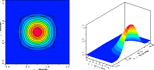
In
Fig. 11
we show the aerial image obtained with the vector-valued
approach used for our
imaging module.
Conventional I-line illumination with a
numerical aperture of
NA = 0.5 and a partial coherence factor of
![]() was used. Nine mutually incoherent point sources were needed to account for
the partial coherence. The point source location is shown
in the wavevector diagram of
Fig. 5.
was used. Nine mutually incoherent point sources were needed to account for
the partial coherence. The point source location is shown
in the wavevector diagram of
Fig. 5.
In
Fig. 12
contour plots of the PAC are shown in the
upper two figures and the developed photoresist profiles
in the lower two figures.
The contours are given for
PAC = ![]() .
The exposure-dose was
.
The exposure-dose was
![]() and the development time was
and the development time was
![]() .
The simulation parameters were for the Dill-model
.
The simulation parameters were for the Dill-model
![]() ,
,
![]() ,
,
![]() ,
,
![]() and for the Kim-model
and for the Kim-model
![]() ,
,
![]() ,
,
![]() (cf. Table IV in [19]).
(cf. Table IV in [19]).
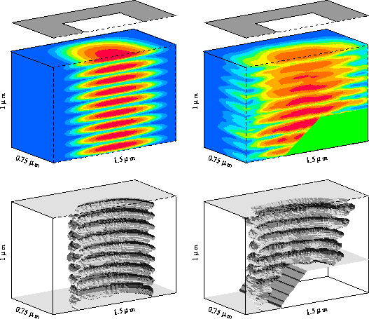
The oval contours are caused from standing waves within
the photoresist, which result from substrate reflections.
Due to the lateral variation in optical thickness
the regular shaped bulk image and
resist profile of the planar topography is distorted
in case of the stepped topography.
Futhermore, the opening for the stepped substrate
is wider than for the planar substrate.
Hence, the effective diameter of the contact hole
depends on the nonplanarity of the wafer topography.
Further comparisons with experiments are not given as the main scope of this paper is to present the overall three-dimensional lithography simulator and to demonstrate its applicability for rigorous three-dimensional workstation based simulation. The intrinsic physical correctness of the various simulation models has already been demonstrated elsewhere (e.g., for the imaging and exposure/bleaching module in [7] and for the development module in [11]) and can therefore be taken as granted.