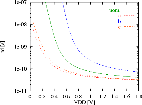
Table 4 shows results from a
pocket-implanted LDD NMOS device with
Lnom= 0.18![]() m,
tox= 5nm, and
Xj= 0.09
m,
tox= 5nm, and
Xj= 0.09![]() m
designed for operation at
VDD= 1.5V.
The system parameters used for analysis were
ld= 7 and a= 0.1
(interconnect capacitances were not
considered).
The evaluation was carried out
for the nominal case (`nominal') and two worst-case corners
(`a':
T=Tmax=125
m
designed for operation at
VDD= 1.5V.
The system parameters used for analysis were
ld= 7 and a= 0.1
(interconnect capacitances were not
considered).
The evaluation was carried out
for the nominal case (`nominal') and two worst-case corners
(`a':
T=Tmax=125![]() C,
channel and pocket implant doses, and L reduced by 20%; and
`b':
T=Tmin=0
C,
channel and pocket implant doses, and L reduced by 20%; and
`b':
T=Tmin=0![]() C,
channel and pocket implant doses increased by 50%,
and L increased by 20%).
The data `c' are the same as `a' except that tox was reduced
instead of the channel and pocket implants (to obtain the same shift
in VT,lin).
Each of these evaluations takes a CPU time of about 5 minutes on an
HP735 workstation.
The errors of the inverter gain and noise margins were determined from
device-level simulations of an inverter with MINIMOS-NT and are
typically in the order of 5%.
C,
channel and pocket implant doses increased by 50%,
and L increased by 20%).
The data `c' are the same as `a' except that tox was reduced
instead of the channel and pocket implants (to obtain the same shift
in VT,lin).
Each of these evaluations takes a CPU time of about 5 minutes on an
HP735 workstation.
The errors of the inverter gain and noise margins were determined from
device-level simulations of an inverter with MINIMOS-NT and are
typically in the order of 5%.
| case | VT,lin | td 1 | Es | fc,max | NM | Ainv | |
| [V] | [ps] | [fJ] | [GHz] | [Vdd] | |||
| nominal | 0.44 | 47.6 | 18.1 | 3.0 | 8.5e4 | 0.36 | 9.7 |
| a: |
0.21 | 34.2 | 27.2 | 4.2 | 7.3e0 | 0.29 | 6.1 |
| b: |
0.67 | 92.6 | 19.3 | 1.5 | 2.6e9 | 0.44 | 34.2 |
| c: |
0.23 | 35.9 | 19.8 | 4.0 | 7.1e1 | 0.32 | 9.9 |
| error | -2.7% | 3.6% |
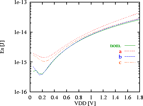
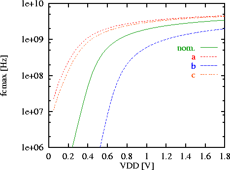
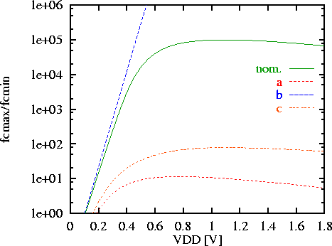
The curves in Figs. 7-10 are the
inverter delay,
switching energy,
maximum clock frequency, and
clock frequency margin fc,max/fc,min
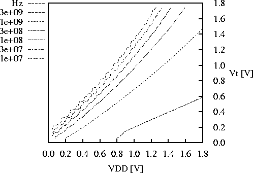
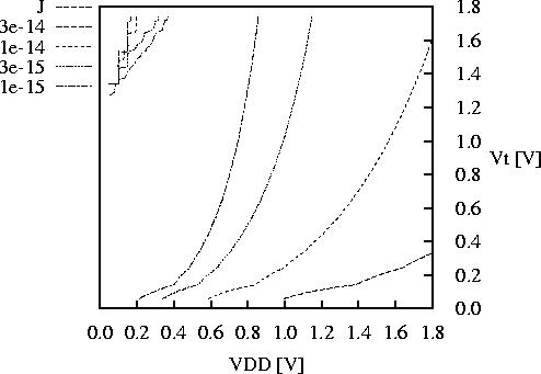
The impact of supply and threshold voltage
on maximum clock frequencyand switching energyis shown in
Figs. 11 and 12.
For the simulations tox was varied from
1nm to 18nm, and fc,max and Es were plotted over
VDD and the extracted VT,lin.
To find an optimum device, one can, e.g., pick a contour
in Fig. 11 according to the required performance
and then, along this contour, find the minimum Es in
Fig. 12.
![]()
![]()
![]()
Next: 9 Conclusion
Up: VLSI Performance Metric Based
Previous: 7 Noise Margins, Inverter
G. Schrom, V. De, and S. Selberherr: VLSI Performance Metric Based on Minimum TCAD Simulations