6.5 Results on Trap-Assisted Tunneling
In 2012 Toledano et al. [159] showed that there is a correlation between gate and drain current
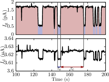
fluctuations in MOSFETs. Figure 6.23 shows a portion of the experimental data. Interestingly the
difference between high and low gate current is 80% of the gate current maximum and temperature
independent. Due to the correlation with the drain current it is concluded that the charged trap
significantly changes the tunneling current. A possible explanation is that the charged
trap changes the local potential such that the number of charge carriers, which tunnel
through the oxide, is reduced by 80%. This would also explain the temperature independence
of the reduction, inherent in direct tunneling. Another explanation is that the tunneling
current is a trap assisted NMP process. In [160] we explored whether the experimental
data could be reproduced by assuming that an occupied trap reduces the direct tunneling
current by purely electrostatic interaction. To assess whether or not this is correct, we first
simulated the electrostatics of the n-channel MOSFET. For this we used the 3D density
gradient and drift diffusion simulator MinimosNT and additionally considered random
dopants. The simulations were done per device, once without and once with a single discrete
trapped charge in the oxide (cf. Chapter 5). Our sample size consisted of 201 microscopically
different devices, i.e. different dopant positions. Then 1D potential profiles (normal to the
semiconductor-oxide interface) were extracted in 1nm increments. These profiles were then
loaded into our NEGF (cf. Chapter 2) simulator, VSP [51], in order to calculate the
relative change in the gate current (direct tunneling) ΔIg∕Ig. The relative tunneling current
change ΔIg∕Ig was obtained by comparing the tunneling currents for the devices without
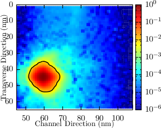
trap to the devices with trap. In Figure 6.24 (left) a normalized map of the local ΔIg∕Ig
over the whole gate area is shown. The map shows high local changes in the vicinity of
the trap. However, as the histogram in Figure 6.24 (right) shows, we could hardly find a
dopant-trap configuration for which the total change in tunneling current exceeded 1%.
This is in stark contrast with the experimentally reproducibly found decrease of 80% in
Ig.
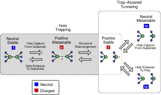
Thus trap-assisted tunneling in the context of the presented four-state NMP model has been
(successfully) explored [161]. Extending the four-state NMP model (cf. Figure 6.25) by taking
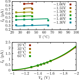
interactions with the poly-gate into account, the experimental data could be reproduced (cf. Figure
6.26). In this extended model one has to differentiate whether the charge carrier to be trapped
originated from the poly-gate or the substrate. Nevertheless, the basic rate equations do not change.
However, the source of the quantities and the tunneling distances are different. In order to
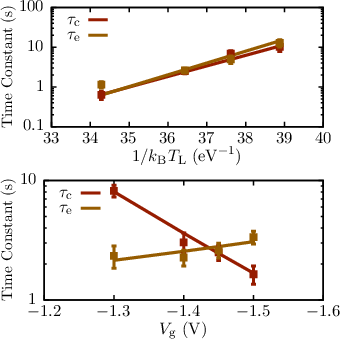
correctly evaluate the capture τc and emission times τe for the trap-assisted tunneling
current the charge state (whether or not the defect is charged) in the modified model had
to be taken into account. In the course of the evaluation of the five-state NMP model
it was found that the weak temperature dependence of the time constants is due to the
weak electron-phonon coupling (small NMP transition barriers) needed to reproduce the
measurement data (cf. Figure 6.26 right top). For details on the model, the reader is referred to
[161].