6.4 Model Evaluation on pMOSFETs using the Direct Current Current Voltage Method
In this section a comparison of the SRH model and the four state NMP model using direct
current current voltage (DCIV) experiments at various temperatures, conducted using the
polyheater technology [153], will be presented. To this end p-type metal-oxide-semiconductor
field-effect transistors (pMOSFETs) are studied using the DCIV method before and after bias
temperature stress. The ability of the SRH model and the four state NMP model to meaningfully
reproduce the acquired DCIV data is compared. It is demonstrated that the SRH model cannot
capture the detailed features of the data and that the more detailed four state NMP model is
required.
6.4.1 Experimental Setup
For the measurement pMOSFETs with 30 nm thick silicon-dioxide as gate dielectric have been used.
All pMOSFETs have been integrated with the polyheater technology presented in [153] in order to be
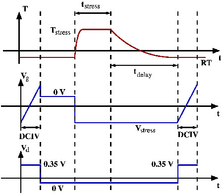
able to locally heat the devices up to 500°C. To monitor the stress induced degradation, DCIV
experiments [127, 128] were performed on fresh devices before and after stress using a drain voltage
V d of 0.35 V to forward bias the pn junctions. For each stress temperature a fresh device was stressed
for ts = 10s by applying a gate voltage of -20 V (V s = -20V and Eox ≈ 6.7MV∕cm). After 10s of
stress the devices were cooled down for tdelay = 200s to room temperature at a gate voltage of -20 V
(cf. Figure 6.15) in order to minimize the relaxation during cool down [154] (degradation
quenching). With the end of the cool down phase a DCIV curve for the stressed device was
recorded.
6.4.2 Comparison of SRH and the four State NMP Model
The standard SRH model for interface traps and the previously introduced four state NMP model for
BTI were used to describe the measurement data in order to compare their ability to reflect the
(N)BTI stress dependent DCIV data. For the extraction all recombination centers, i.e. stress induced
defects, were assumed to be at or near the silicon-oxide interface. During DCIV experiments the bulk
current is directly proportional to the number of recombination events [127], simplifying the analysis
considerably. It is important to note that any carrier recombination in the bulk, especially at the pn
junctions, would cause a constant bulk current during the DCIV experiment. Since we did not observe
a shift of the measured DCIV curves along the ordinate within the accuracy of the measurement
equipment we can safely assume negligible carrier recombination in the bulk. Geometrical
effects could be safely neglected, since large devices with a 30 nm thick gate dielectric and a
nominal gate length larger than 100 nm were used. To assess the ability of the SRH model to
reflect the DCIV measurement data, the formula originally derived in [155] was used. It
reads
| R | = 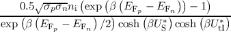 , , | (6.51)
|
| US* | = ϕ
s + ln - - ∕2, ∕2, | (6.52)
|
| UTI* | =  ln ln , , | (6.53) |
where ni is the intrinsic carrier concentration, EFn and EFp are the quasi Fermi levels for
electrons and holes respectively, Ei is the intrinsic energy, σp and σn are the constant
hole and electron capture cross sections, ϕs is the surface potential, and β = (kBTL)-1.
In the analysis transitions from/to state 1′ are neglected to obtain a simplified approximation to the
full model. Further it was assumed that the DCIV experiment itself does not stress the device any
further. This assumption was experimentally justified by comparing DCIV curves for various
measurement durations, i.e. different slopes of the gate voltage applied, whereas the measurements
yielded the same DCIV curves. With the stated simplification the derivation of a compact analytical
version of the carrier recombination rate for the multistate NMP model can be undertaken. By
defining effective rates the three remaining defect states have been reduced to only two equvialent
states. The effective rates are [156],
k12 =  andk21 = andk21 =  . . | | (6.54) |
Employing Maxwell-Boltzmann statistics and applying the assumptions discussed above to the
first-order differential for the four state NMP model one obtains
| ∂tf = k21(1 - f) - k12f = 0, | | (6.55) |
for the occupancy of a trap. Using the definition of the recombination rate for holes Rp in steady state
and inserting the solution of (6.55), gives an analytical formula in the framework of a multistate NMP
model for carrier recombination
| R | = -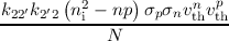 | (6.56)
|
| N | = exp k22′nσnvn
th + exp k22′nσnvn
th + exp k2′2pσpvp
th k2′2pσpvp
th | |
|
| + exp k2′2niσnvn
th k2′2niσnvn
th | |
|
| + exp k22′niσpvp
th, k22′niσpvp
th, | (6.57) |
where vnth and vp
th are the electron and hole carrier velocities, σn and σp are the constant electron
and hole capture cross sections. For all simulations the constant capture cross sections
σn and σp were fixed to a value of 2.0 × 10⁻¹⁶cm2 for the SRH and the multistate NMP
model.
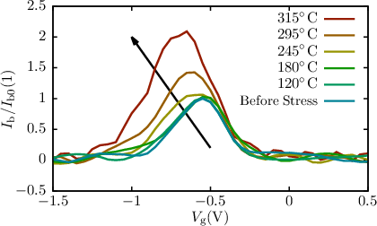
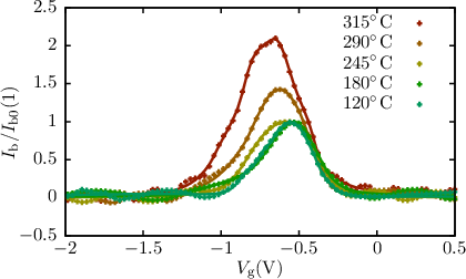
DCIV curves measured for various stress temperatures, which have been normalized to the peak
value for Tstress ≈ 245°C for comparison, are shown in Figure 6.17. The maximum value of the bulk
current Ib increases with higher stress temperatures as expected. Also noteworthy is the broadening of
the bell-shaped DCIV curve towards negative gate voltages, whereas there is almost no broadening
towards positive gate voltages (cf. Figure 6.17 for V g > -0.5V). This indicates that traps with higher
effective activation energies are becoming active trapping centers at higher stress temperatures.
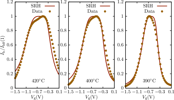
A fit of the SRH model [136] for the post-stress measurement data is shown in Figure 6.18. It can
be seen that the SRH model can reproduce the DCIV curve only for certain stress temperatures (in
this case Tstress ≈ 240°C), but not for a wide range of stress temperatures. Especially for stress
temperatures above 315°C, when the DCIV bell-shaped curve develops a shoulder towards negative
gate voltages, the SRH model cannot reproduce the experimental data as shown in Figure 6.19.
Noteworthy is the fact, as seen in Figure 6.19, that the post-stress DCIV curve changes its shape for
stress temperatures above 315°C. This is why the SRH model, for which the recombination current
exhibits a cosh-1 shape (cf. (6.51)) for all temperatures [155], cannot reproduce the experimental
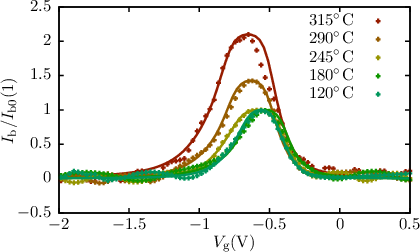
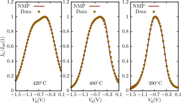
data anymore. In contrast to the SRH model the four state NMP model can give excellent fits to the
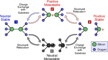
data for all stress temperatures as shown in Figure 6.20. This can be attributed to the fact that the
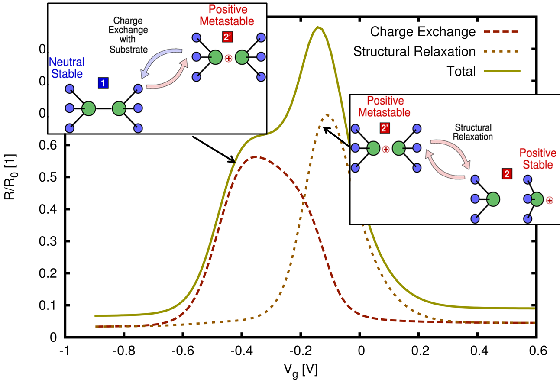
reduced four state NMP model additionally considers structural relaxation (cf. Figure 6.16 and Figure
6.22).
To understand why structural relaxation can explain the additional shoulder above a stress
temperature of 315°C in our data, we reformulated the carrier recombination formulae in
the four-state NMP model (6.56) and for the SRH model (6.52) such that both formulas
have the same structure. The carrier recombination rate for both models has the following
structure
| R | = -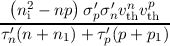 , , | (6.58) |
where τ′n and τ′p are the carrier lifetimes for electrons and holes and σ′n and σ′p are the capture cross
sections for electrons and holes, respectively. These parameters are model-dependent. For the SRH
model the capture cross sections have fixed values, where
| σ′n = σn = 2.0 × 10⁻¹⁶cm2, | | (6.59)
|
| σ′p = σp = 2.0 × 10⁻¹⁶cm2. | | (6.60) |
In contrast, the four-state NMP model gives
| σ′n | =  σn = σn = 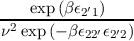 σn, σn, | (6.61)
|
| σ′p | =  σp = σp =  σp. σp. | (6.62) |
Furthermore, the carrier lifetimes differ strongly between the SRH model and the multistate NMP
model [151]. Thus it can be stated that the effective capture cross sections of the multistate NMP
model are device temperature, oxide field and parameter dependent, while those of the SRH model are
always constant. By adjusting the energy barriers (ϵ22′ and ϵ2′2) describing the structural relaxation
(cf. Figure 6.9 and Figure 6.16) it is possible to perfectly fit the DCIV curves measured after high
temperature stress (cf Figure 6.21). Figure 6.22 depicts how the shoulder, for stress temperatures
above 315°C, can be described using a multistate NMP model. If structural relaxation is
neglected (cf state 2 in Figure 6.16) one obtains a standard NMP model [157, 158]. For the
standard NMP model the energy barriers (ϵ22′ and ϵ2′2) describing the structural relaxation
are zero. Thus the effective capture cross sections of the standard NMP model reduce
to
σ′n =  σn = exp σn = exp σn and σ′p = σn and σ′p =  σp = exp σp = exp σp. σp. | | (6.63) |
This reduction of the multistate NMP model results in a less pronounced temperature dependence
[29] and in the loss of two degrees of freedom for parameter extraction.
The investigation of the capability of the SRH and NMP model to explain DCIV measurements of
pMOS devices after NBTI stress at various stress temperatures shows the importance
of structural relaxation for a proper description of recombination currents. A moderate
agreement between model and measurement data could be obtained with the conventional SRH
model.