|
|
|
|
Previous: B.2.4 BOUNDARIES Section Up: B.2 Definition of the WSS Grammar Next: B.3 Definition of the Config File Grammar. |
|
|
|
|
Previous: B.2.4 BOUNDARIES Section Up: B.2 Definition of the WSS Grammar Next: B.3 Definition of the Config File Grammar. |
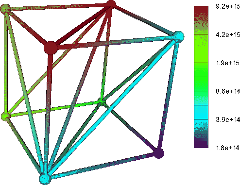
The following sample WSS file is given as a reference to further illustrate the syntax. The example describes a Wafer with the geometry and attribute of the cube depicted in Fig. B.8, a segment named Bulk with an attribute Acceptors and a property MaterialType, and a boundary named Contact.
|
VERSION "1.4"
NAME		Hbt
DIMENSION	3
POINTS
{ 0.000000e+00 0.000000e+00 1.000000e+00
  1.000000e+00 0.000000e+00 0.000000e+00
  1.000000e+00 1.000000e+00 1.000000e+00
  1.000000e+00 0.000000e+00 1.000000e+00
  1.000000e+00 1.000000e+00 0.000000e+00
  0.000000e+00 1.000000e+00 1.000000e+00
  0.000000e+00 0.000000e+00 0.000000e+00
  0.000000e+00 1.000000e+00 0.000000e+00
}

SEGMENTS
{ Bulk
  {  ATTRIBUTES
    {  GRID Acc_Grid
      { 0 1 2 3
        4 0 1 2
        0 4 5 2
        6 4 0 1
        4 7 0 5
        4 7 6 0
      }

      Acceptors         # attribute named Acceptors
      { GRID Acc_Grid   # attribute is defined on grid named Acc_Grid
        3.907985e+14
        9.853947e+14
        4.163100e+14
        1.766426e+14
        9.133061e+15
        9.229765e+15
        3.646022e+15
        4.872172e+15
      }

      MaterialType_1
      { "Silicon"
      }
    }

    BOUNDARIES                    # Boundaries section (optional)
    {
      GRID Contact_Grid           # a grid named Contact_Grid
      {
        0 1 2
        0 2 3
      }

      Contact
      {
        GRID Contact_Grid
      }
    }
  }
}
2003-03-27