In the following, two implantation simulations that were performed
with MCIMPL are presented. The input structure for the first example is shown
in Fig. 4.1. It
Figure 4.1:
CMOS structure for well and threshold adjust implantation
examples. The green region is silicon. The gray region depicts the gate oxide
and the shallow trench isolation (STI).
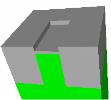 |
displays one half of a schematic transistor structure. The cut through the
transistor is along the gate such that the drain and half of the gate region is
visible. The shallow trench isolation (STI) is already present in the
depicted structure. In Fig. 4.2 a well implant is shown. This
implants are used to build the n-well for a typical CMOS
process. Fig. 4.3 depicts a shallow implant (low energy) as it
is typically used to adjust the threshold voltage  of a
MOS transistor. This implant was also performed into the input
structure depicted in Fig. 4.1.
of a
MOS transistor. This implant was also performed into the input
structure depicted in Fig. 4.1.
Figure 4.2:
Front and back view of a
well implant that was performed at an energy of  keV, a tilt angle of
 , a dose of
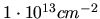 and with the dopant species
boron.
and with the dopant species
boron.
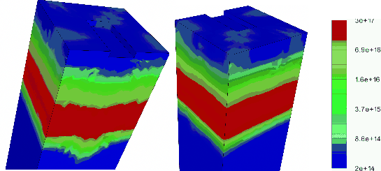 |
Figure 4.3:
Front
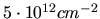
and back view of a threshold voltage adjust implant at an energy of  keV,
a tilt angle of , a dose of
keV,
a tilt angle of , a dose of
 and with the
dopant species boron.
and with the
dopant species boron.
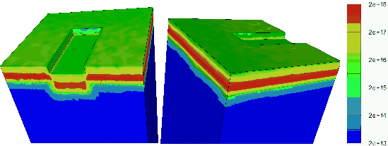 |
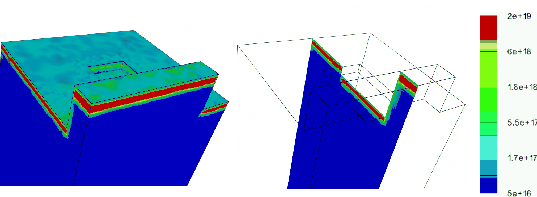
Fig. 4.4 depicts the input for the second
implantation example. The structure is in principle similar to the first one but
the polysilicon gate is already formed and serves as a mask.
A technique to reduce the leakage
current of a MOS transistor is to reduce the field in the junction region by
introducing a lightly doped drain (LDD) implant. Fig. 4.5 depicts
such an LDD implant.
Figure 4.4:
CMOS structure
for LDD implantation example. The green region is silicon. The gray region
depicts the oxide and the red region is polysilicon.
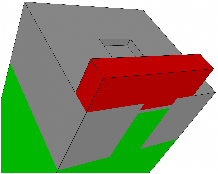 |
Figure 4.5:
LDD implant at an energy of keV, a tilt angle of
, a dose of
 and with the dopant species
phosphorus.
and with the dopant species
phosphorus.
 |
2003-03-27