The description of the time period up to void nucleation must be directly followed by a model which handles void evolution.
Once a void is nucleated, material transport on the void metal interface dominates [54,64,60,61,63].
The driving forces are electromigration proportional to the local tangential component of the electric field and the chemical potential.
Since the most critical voids are nucleated at the copper/barrier and copper/cap-layer interfaces, which also represent the fastest diffusion paths, available models [64,60] have to be extended in order to include these phenomena.
Void evolution was originally handled applying explicit void surface tracking methods [64]. A further development was introducing numerically efficient diffuse interface models [56,57,58,59].
However, not until introducing an adaptive mesh approach into the diffuse interface method [62], realistic interconnect structures could be handled.
Applying a diffuse interface model we are able to predict the intrinsic void behavior from the nucleation until failure. The simulation of the evolving void/metal interface is accompanied with electrical field calculation and resistance extraction.
Once the void is nucleated, the dominating factor for the void evolution is the self-diffusion on the void surface and in the vicinity of this surface. The driving forces are again the chemical potential and the tangential component of the electrical field gradient. The chemical potential in this case is comprised of components due to the free energy of the surface and the local elastic strain energy. The material is transported along the void surface and into the metal bulk. This effect gives rise to the movement of the whole void and it's shape change. In this context the crystal orientation must be considered because of the anisotropic characteristics of self-diffusion [54].
Since the problem is a moving boundary problem, the first attempts to handle it was the application of explicit tracking of the void/metal interface by means of finite element methods [64,60].
These methods are quite complicated to implement and also have rather poor numerical stability.
To overcome the problems mentioned above, we apply a diffuse interface model.
In a diffuse interface model void and metal area are presented through an
order parameter ![]() which takes values
which takes values ![]() in the metal area,
in the metal area, ![]() in
the void area and
in
the void area and
![]() in the void-metal interface
area.
Demanding explicit tracking of the void-metal interface is not needed and models do not require boundary conditions to be enforced at the moving boundary.
in the void-metal interface
area.
Demanding explicit tracking of the void-metal interface is not needed and models do not require boundary conditions to be enforced at the moving boundary.
The evolving void/metal interface is described through the time dependent distribution of the order parameter ![]() .
The actual diffuse interface is a belt area around the iso-surface
.
The actual diffuse interface is a belt area around the iso-surface ![]() .
This belt area has some finite width.
With shrinking width of this belt area the accuracy of the simulation increases.
The diffuse interface governing equation (DIGE) is a central part of each diffuse interface based modeling.
The equation itself comprises electromigration and stress driven material transport on the void/metal interface and on this basis regulates the distribution of the order parameter.
This equation is an extension of the well-known Chan-Hilliard equation [56,57,58,85,86].
Concerning the solution of Chan-Hilliard type equations several approach are proposed in the literature [85,86].
The gap between fast and reliable DIGE solving approaches which are already known from the literature and a solution approach which is also applicable for arbitrary interconnect geometries was bridged by introducing an adaptive grid technique [62].
.
This belt area has some finite width.
With shrinking width of this belt area the accuracy of the simulation increases.
The diffuse interface governing equation (DIGE) is a central part of each diffuse interface based modeling.
The equation itself comprises electromigration and stress driven material transport on the void/metal interface and on this basis regulates the distribution of the order parameter.
This equation is an extension of the well-known Chan-Hilliard equation [56,57,58,85,86].
Concerning the solution of Chan-Hilliard type equations several approach are proposed in the literature [85,86].
The gap between fast and reliable DIGE solving approaches which are already known from the literature and a solution approach which is also applicable for arbitrary interconnect geometries was bridged by introducing an adaptive grid technique [62].
The main idea of the adaptive grid method was to use local grid refinement and a coarsening algorithm, a fine grid is set dynamically adjusted only in the vicinity of the void/metal interface. The geometry of the interconnect can be arbitrary and, due to the economical distribution of the grid density, computation can be performed efficiently.
Additional equations to be solved such as the Laplace equation for the electric field and mechanical stress-strain model equations are adapted to the diffuse interface model through an order parameter dependence of the electrical conductivity and the elastic compliance [59]. These equations are solved using common finite element schemes assuming a finite width of the diffuse interface area. Generally the accuracy of the calculation will increase by reducing this width. There is a rigorous asymptotic theory which proves that the diffuse interface model converges to the sharp void/interface physical situation both in the equations' solution and in the compliance with boundary conditions [56,57,58,59].
The initial void is placed on the spot predicted by the first stage module and the second stage module is invoked, which simulates evolution of the void under the impact of driving forces, until it reaches a critical size which changes the initial interconnect resistivity to such an extent that it can be considered as actual interconnect failure.
Thereby the resistance change up to the interconnect failure and, the time needed for this failure to occur are provided.
We call this time period void evolution time and added to the void nucleation time calculated in the first stage module, it defines the interconnect time to failure.
We assumed unpassivated monocrystal isotropic interconnects where
stress phenomena can be neglected.
An interconnect is idealized as two-dimensional electrically
conducting via which contains initially a circular void. For simplicity we also neglect the effects of grain boundaries and lattice diffusion.
In this case there are two main forces which influence the shape of
the evolving void interface: the chemical potential gradient and
electron wind.
The first force causes self-diffusion of metal atoms on
the void interface and tends to minimize energy which results in
circular void shapes.
The electron wind force produces asymmetry in
the void shape depending on the electrical field gradients.
Including contributions from both, electromigration and chemical
potential-driven surface diffusion, gives the total surface atomic
flux,
![]() =
=
![]() , where
, where ![]() is the unit vector
tangent to the void surface [60,87]
is the unit vector
tangent to the void surface [60,87]
 exp exp |
(4.42) |
| (4.43) |
| (4.47) |
The diffuse interface model equations for the void evolving in an unpassivated
interconnect line are the balance equation for the order parameter ![]() [56,57,58,59],
[56,57,58,59],
The equations (4.48)-(4.50) are solved by means of the finite element method on a
sequence of the grids
![]() each one adapted to the position of the
void-metal interface from the previous time step. The initial grid
each one adapted to the position of the
void-metal interface from the previous time step. The initial grid
![]() is produced by refinement of some basic triangulation
is produced by refinement of some basic triangulation ![]() of area
of area ![]() according to the initial profile of order parameter
according to the initial profile of order parameter ![]() .
The motivation of grid adaptation is to construct and maintain a fine
triangulated belt of width
.
The motivation of grid adaptation is to construct and maintain a fine
triangulated belt of width
![]() in the interconnect area
where
in the interconnect area
where
![]() , respectively, where the void-metal interface area is placed.
, respectively, where the void-metal interface area is placed.
| (4.52) |
![]() is a triangulation of the area
is a triangulation of the area ![]() at discrete time
at discrete time ![]() , and
, and
![]() are discrete nodal values of the order parameter on this triangulation.
A finite element based iteration for solving (4.48)
on grid
are discrete nodal values of the order parameter on this triangulation.
A finite element based iteration for solving (4.48)
on grid
![]() and evaluating the order parameter at the
time
and evaluating the order parameter at the
time
![]() consists of two steps [88]:
consists of two steps [88]:
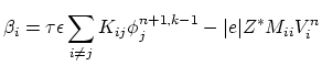
Step 1. For the ![]() iteration of the
iteration of the ![]() time step
the linear system of equations has to be solved:
time step
the linear system of equations has to be solved:
 |
(4.54) |
 |
(4.55) |
| (4.57) |
After an order parameter was evaluated on the
![]() a
grid needs to be adapted according to the new void-metal interface
position.
Therefore it is necessary to extract all elements which are cut by
the void-metal interface in grid
a
grid needs to be adapted according to the new void-metal interface
position.
Therefore it is necessary to extract all elements which are cut by
the void-metal interface in grid
![]() .
The following
condition is used: We take a triangle
.
The following
condition is used: We take a triangle
![]() and denote its vertices as
and denote its vertices as
![]() . The triangle
. The triangle ![]() belongs to the interfacial
elements if for the values of the order parameter
belongs to the interfacial
elements if for the values of the order parameter ![]() at the triangle's
vertices holds
at the triangle's
vertices holds
![]() or
or
![]() . We assume that an interface intersects each edge of the element only once.
The set of all interfacial elements at the time
. We assume that an interface intersects each edge of the element only once.
The set of all interfacial elements at the time ![]() is denoted as
is denoted as
![]() . The centers of gravity of each triangle from the
. The centers of gravity of each triangle from the ![]() build the interface point list
build the interface point list ![]() .
The distance of the arbitrary point
.
The distance of the arbitrary point ![]() from
from ![]() is defined as,
is defined as,
| (4.59) |
The grid adaption algorithm used in this work is a version of
the algorithm introduced in [89] and consists of a grid
refinement algorithm and a grid coarsening algorithm.
The refinement algorithm is based on recursive bisecting of
triangles. A triangle is marked for refinement if it complies with
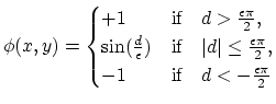
some specific refinement criterion ![]() . In our application we used
. In our application we used
![]() for the initial refinement and
for the initial refinement and ![]() for the grid
maintaining refinement. For every
triangle of the grid, the longest one of its edges is marked
as refinement edge.
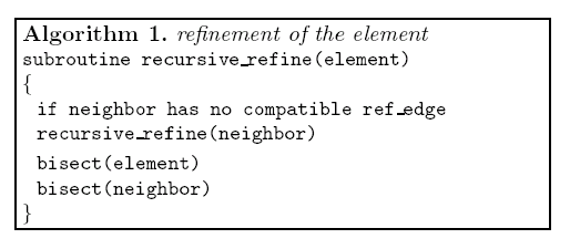
The element and its neighbor element which also contains the same refinement edge are refined by bisecting this
edge (Fig. 4.6). We can define refinement of the element in
the following way:
for the grid
maintaining refinement. For every
triangle of the grid, the longest one of its edges is marked
as refinement edge.
The element and its neighbor element which also contains the same refinement edge are refined by bisecting this
edge (Fig. 4.6). We can define refinement of the element in
the following way:
Now, the overall refinement algorithm can be formulated as follows:
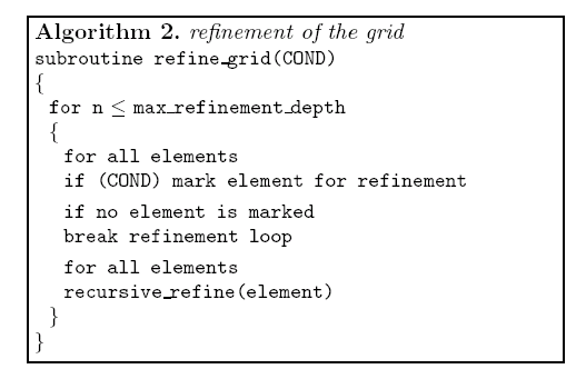
The parameter max_refinement_depth limits the number of
bisecting of a triangle.
The grid is refined until there is no more element marked for refinement or the maximal refinement
depth is reached.
The coarsening algorithm is more or less the inverse of the refinement
algorithm. Each element that does not fullfil criterion ![]() is
marked for coarsening. The basic idea is to find the father element whose refinement
produced the element in consideration.
is
marked for coarsening. The basic idea is to find the father element whose refinement
produced the element in consideration.
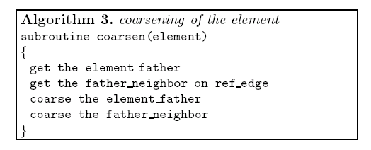
The following routine coarsens as many elements as possible, even more than once if allowed:
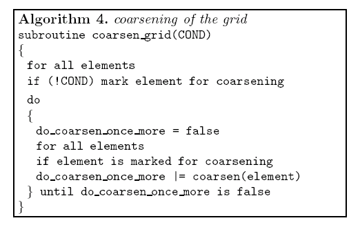
The complete adaption of the grid is reached by sequential invoking of the grid refinement and of the grid coarsening algorithm.
![\includegraphics[width=0.7\linewidth]{figures/refine.eps}](img879.png)
![\includegraphics[height=0.7\linewidth]{figures/solving.eps}](img883.png)