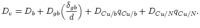
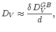
In the case of copper interconnects there are several types of vacancy diffusivities of importance, namely, diffusion in the bulk material, grain boundary diffusion, the diffusion along the copper/barrier interfaces, and the diffusion along copper/cap-layer interface.
The bulk diffusion coefficient can be neglected for temperatures well below the melting point [55].
The simpliest way to take into account all diffusivities is by introducing an effective diffusion coefficient dependent on the diffusivity coefficients of all paths and on microstructural parameters such as grain size and grain boundary thickness [77].
Since most copper grains in a Damascene lines are not larger than 0.3 ![]() m the majority of the interconnects used today will inevitably have a bamboo structure, so that averaging in the sense of an effective diffusion coefficient is feasible.
However, fast diffusivity paths along copper/barrier and copper/cap-layer interfaces will influence the vacancy dynamics strongly depending on the specific interconnect layout.
This influence can not be incorporated with simple averaging terms. The diffusivity must be a cumulative value as used in [55]
m the majority of the interconnects used today will inevitably have a bamboo structure, so that averaging in the sense of an effective diffusion coefficient is feasible.
However, fast diffusivity paths along copper/barrier and copper/cap-layer interfaces will influence the vacancy dynamics strongly depending on the specific interconnect layout.
This influence can not be incorporated with simple averaging terms. The diffusivity must be a cumulative value as used in [55]
To predict the location of the void nucleation sites and the time needed for a void to nucleate a multitude of microstructural, chemical, process-related, and environment-related variables have to be taken into account.
The microstructural characteristics which need to be considered are the grain boundary structure and the orientation of the crystal axes inside the grains.
Numerous experiments [55,8] have shown that the design of the interconnect, passivation, and barrier layers, together with the material composition of these layers, has a significant impact
on the localization of void nucleation sites.
Of crucial importance for the void-nucleating condition are the dynamics of the crystal vacancies of the interconnect metal. Depending on crystal texture of the used copper interconnect and it's geometry there are several possible paths for the vacancy diffusion.
The coupling of the vacancy dynamics with the stress development was first introduced by Korhonen in [51]. The analysis was carried out for a passivated straight aluminum interconnect line with a columnar grain structure with the grain boundaries perpendicular to the substrate. The author assumes that vacancy diffusion along grain boundaries equilibrates the stress in such a way that it reduces to a hydrostatic state on a time scale that is short compared to that for long range diffusion along the entire line length. The recombination and generation of vacancies changes the concentration of the available lattice sites, which consequently influences the hydrostatic stress distribution. Specifically, the loss of the available lattice sites yields an increase of the hydrostatic stress.
This assumption greatly simplifies the analysis und allows an analytical solution of the governing equation. However, this approach is eglible only for passivated straight interconnects with a specific aluminum crystal texture.
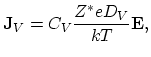
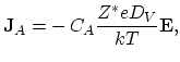
Metal self-diffusion occurs via a vacancy exchange mechanism. The atomic flux
![]() is equal and opposite the flux of vacancies
is equal and opposite the flux of vacancies
![]() . Therefore, the electromigration induced vacancy flux resulting from an applied electric field
. Therefore, the electromigration induced vacancy flux resulting from an applied electric field
![]() is given by [51],
is given by [51],
One of the basic assumptions made by Korhonen [51], is that electromigration will deposit atoms in grain boundaries in such a way that mechanical stress very fast becames uniform (compared with the self-diffusion along the interconnect) at a any particular cross section of straight interconnect (perpendicular to the electrical current direction). This assumption significantly simplifies analysis because the mechanical stress gradient is non-zero only in the electrical current direction where it opposites electromigration.
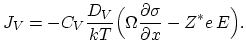
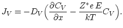
The model transport equations can be expressed in terms of either vacancies or atoms but in most cases [51] vacancy are chosen. The net vacancy flux along the length of the interconnect line induced by the gradient of the chemical potential and electromigration, taking into account (4.16) can be written as,
Instead of an intermediate relationship between the density of lattice sites and hydrostatic stress other researchers [81,82] employed the idea that the vacancy diffusion flux gives rise to volumetric strain which serves to establish stress fields, driving stress migration fluxes. This approach is utilized in [70]. The main advantage is that one does not need the assumption of local stress-vacancy equilibrium, the elastic behavior of metal is not required, and most important, all components of the stress tensor are included. Thus arbitrary geometric shapes in connection with the complex mechanical boundary conditions can be investigated.
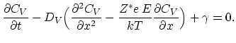
Korhonen's equation can be analytically solved for different cases of initial and boundary conditions [51,7,80,83], however from the practical point of view, the most important solution is for the situation where the vacancy flux is blocked at the both ends of a finite line, i.e.
 |
(4.27) |
|
|
 |
(4.28) |
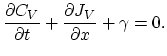
According to the discussion presented in [50], the sink/source term ![]() models the interaction of vacancies between the grain boundary and the grain.
The vacancies are annihilated or produced inside the grain boundaries with a rate
models the interaction of vacancies between the grain boundary and the grain.
The vacancies are annihilated or produced inside the grain boundaries with a rate ![]() which depends on the vacancy concentration in the vicinity of the grain boundaries [50],
which depends on the vacancy concentration in the vicinity of the grain boundaries [50],
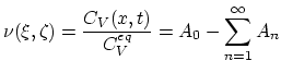
Today a semi-empirical model equation (4.5) is widely used to extrapolate interconnects' time to failure under accelerated test conditions compared to operating conditions.
Based on experimental observations [3], the value of the current density exponent ![]() in (4.5) is found to be
in (4.5) is found to be ![]() for the nucleation failure mechanism in which failure is dominated by the time required to build-up a critical stress or a critical vacancy concentration.
For the void-growth mechanism, in which failure is determined by the growth of the void to the critical size, the current density exponent is
for the nucleation failure mechanism in which failure is dominated by the time required to build-up a critical stress or a critical vacancy concentration.
For the void-growth mechanism, in which failure is determined by the growth of the void to the critical size, the current density exponent is ![]() .
.
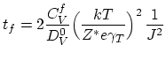
Considering the nucleation failure mechanism for arbitrary given critical vacancy concentration ![]() , Shatzkes and Lloyd [80] derived following the equation for the time to failure,
, Shatzkes and Lloyd [80] derived following the equation for the time to failure,
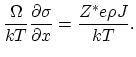
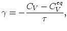
Based on the model propositions in [50] Sarychev et al. [70] developed a new model which can be easier applied to realistic interconnect structures. The model connects the evolution of the stress tensor with the diffusion of vacancies whereas the influence of the geometry of the metalization is included. The cause of the stress is the local volume change which is generated by vacancy migration and generation due to electromigration. This mechanical stress opposes electromigration driven vacancy migration. The additional stress load to be included stems from residuum stress as result of the technological process and from mechanical stress due to the thermal mismatch between copper, barrier, and the passivation layer.
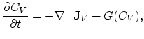
The crucial importance for the void-nucleating condition is the dynamics of vacancies in the interconnect metal. The behavior of vacancies can be basically described by the following two equations [7,70],
Local vacancy migration and generation gives rise to the local volume deformation described by the kinetic relation,
There has been some difference between the understanding of this sink/source function ![]() in the Sarychev model [70,84] and models developed on the basis of Korhonen's work [51,7].
Korhonen [51] assumes that the sink/source function represents the interaction of vacancies between the grain boundary and the grain: annihilation of grain boundary vacancies if their concentration is larger than equilibrium concentration, and their production in the opposite case (Section 4.4.3).
On the other hand, Sarychev [70] makes the sink/source term independent of the crystal texture and states that recombination/annihilation takes place everywhere in the bulk.
in the Sarychev model [70,84] and models developed on the basis of Korhonen's work [51,7].
Korhonen [51] assumes that the sink/source function represents the interaction of vacancies between the grain boundary and the grain: annihilation of grain boundary vacancies if their concentration is larger than equilibrium concentration, and their production in the opposite case (Section 4.4.3).
On the other hand, Sarychev [70] makes the sink/source term independent of the crystal texture and states that recombination/annihilation takes place everywhere in the bulk.
The described equation system is already solved analytically for special two-dimensional geometry cases in [70].
In [84] a simple finite element solution of the Sarychev's equations for a two-dimensional 20 ![]() m
m![]() 100
100 ![]() m Al thin film is presented.
m Al thin film is presented.
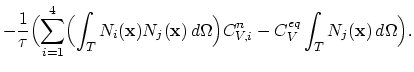
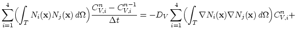
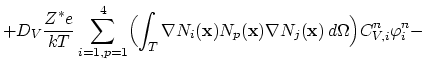
We are going to demonstrate the numerical handling of the basic continuum equation of the Sarychev model. For the sake of simplicity we assume unpassivated interconnects where the stress relaxation to the hydrostatic state is faster than vacancy diffusion, and where the vacancy concentration in the initial phase of electromigration stressing does not deviate from the equilibrium concentration. In that case the vacancy dynamics is described by a three-dimensional Korhonen-type equation,
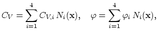
By introducing the spatial discretization of the vacancy concentration ![]() and the electrical potential
and the electrical potential ![]() with the linear basis functions
with the linear basis functions
![]() ,
,
 |
 |
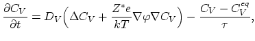
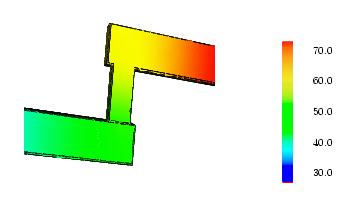
Already a simple electromigration model described by (4.37) enables some insight in the electromigration caused material transport phenomena taking place in the copper interconnect layout. In Figure 4.4 the interconnect via with barrier layer is displayed. Here we can also see the electrical potential distribution which determines the electromigration driving force intensity and direction. The vacancy concentration distribution, obtained by solving equation (4.37), shows a peak value at the bottom of the via (Figure 4.5). This peak concentration region indicates a probable location of void nucleation.
 exp
exp
![$\displaystyle A_n=\frac{16n\pi[1-(-1)^n\text{exp}(\alpha/2)]}{(\alpha^2+4n^2\pi^2)^2}\Bigl(\text{sin}(n\pi\xi)+\frac{2n\pi}{\alpha}\text{cos}(n\pi\xi)\Bigr),$](img757.png)
![\includegraphics[width=\textwidth]{figures/vacancy.eps}](img760.png)
![\includegraphics[width=\textwidth]{figures/stress.eps}](img761.png)
 exp
exp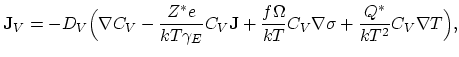
![$\displaystyle \frac{C_V}{C_{V,0}}-(1-f)\Omega\sigma\Bigr],$](img780.png)
![$\displaystyle \frac{\partial \varepsilon^{v}_{kk}}{\partial t}=\Omega[f \nabla \mathbf{J}_V+(1-f)G(C_V)],$](img784.png)