


Next: 2 Estimating the Void
Up: 6 Simulation Results
Previous: 6 Simulation Results
1 Two-Dimensional Void Evolution
In all following simulations a circle was chosen as initial void shape. The
resolution of the parameter  profile can be manipulated by setting
parameter
profile can be manipulated by setting
parameter  which is the mean number of triangles across
the void-metal interface. On Fig. 4.8 initial grids for
which is the mean number of triangles across
the void-metal interface. On Fig. 4.8 initial grids for  and
and
 are presented.
Figure 4.8:
Initial grid refinements.
|
|
We consider a two-dimensional, stress free, electricaly conducting
interconnect via.
Figure 4.9:
Interconnect via with initial void.
|
 constant voltage is applied between points and
 (Figure 4.9). At a refractory
layer is assumed. Because of geometrical
reasons there is current crowding in the adjacencies of the corners
(Figure 4.9). At a refractory
layer is assumed. Because of geometrical
reasons there is current crowding in the adjacencies of the corners
 and
and  .
The analytical solution of equation (4.52) has at these points
actually a singularity [90,76].
.
The analytical solution of equation (4.52) has at these points
actually a singularity [90,76].
High electrical field gradients in the area around the corner points
increase overall error of the finite element scheme for the equation
(4.52) which is overcome by applying an additional refinement of
the basic mesh 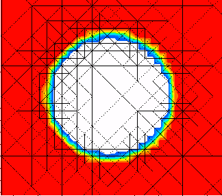 according to the local value of the electric
field gradient (Figure 4.10).
according to the local value of the electric
field gradient (Figure 4.10).
Figure 4.10:
Profile of the current density (in  ) at the corners of
the interconnect.
) at the corners of
the interconnect.
|
A fine triangulated belt area which is attached to the void-metal
interface at the initial simulations step follows the
interfacial area throughout the simulations whereby the interconnect area
outside the interface is coarsened to the level of the basic grid
 (Figure 4.11).
Figure 4.11:
Refined grid around the void in the proximity of the
interconnect corner.
|
Figure 4.12:
Void evolving through interconnect in the electric current direction
|
Figure 4.13:
Time dependent resistance change during void evolution for
the different initial void radius  .
.
|
In our simulations a void evolving through the straight part of the
interconnect geometry exhibits similar shape changes as observed in earlier models [60,59]. There is also no significant
fluctuation of the resistance during this period of interconnect
evolution.
The situation changes when the void evolves in the
proximity of the interconnect corner (Figure 4.12).
Due to current crowding in this
area the influence of the electromigration force on the material transport on the void surface
is more pronounced than the chemical potential gradient. This
unbalance leads to higher asymmetry in the void shape then observed in
the straight part of the interconnect (Figure 4.12).
A void evolving in the proximity of the interconnect corner causes significant
fluctuations in the interconnect resistance due to void asymmetry and
position.
The resistance change shows a charasteristic
profile with two peaks and a valley (Figure 4.13). The extremes are
more pronounced for the larger initial voids.
The capability of the applied adaptation scheme is also presented in the
simulation of void collision with the interconnect refractory layer (Figure 4.14).
The time step  for the numerical scheme
(4.55)-(4.58) is fitted at the simulations begin taking into account
inverse proportionality of the speed of the evolving void-metal interface to the initial void radius [60]:
for the numerical scheme
(4.55)-(4.58) is fitted at the simulations begin taking into account
inverse proportionality of the speed of the evolving void-metal interface to the initial void radius [60]:
 |
(272) |
Figure 4.14:
Grid adaptation in the case of void collision with the refractory layer.
|
 is the characteristical length of via geometry.
An appropriate choice of the time step ensures that the evolving
void-metal interface will stay inside the fine grid belt during the
simulation.
The dynamics of the evolving void-metal interface simulated with a
the presented numerical scheme complies with the mass conservation law,
the void area (where
is the characteristical length of via geometry.
An appropriate choice of the time step ensures that the evolving
void-metal interface will stay inside the fine grid belt during the
simulation.
The dynamics of the evolving void-metal interface simulated with a
the presented numerical scheme complies with the mass conservation law,
the void area (where  ) remains approximately the same during
the whole simulation.
Notable area deviations during the simulation appear only, if a
relatively large factor
) remains approximately the same during
the whole simulation.
Notable area deviations during the simulation appear only, if a
relatively large factor  has been chosen.
As scaling length we took
has been chosen.
As scaling length we took  and for the initial void radius
 ,
,
 , and
, and
 .
Our simulations have shown that for all considered initial void radii,
voids follow the electric current direction (Figure 4.13) and do not transform in slit or wedge like formations which
have been found to be a main cause for a complete interconnect
failure [54].
Already with
.
Our simulations have shown that for all considered initial void radii,
voids follow the electric current direction (Figure 4.13) and do not transform in slit or wedge like formations which
have been found to be a main cause for a complete interconnect
failure [54].
Already with
 good approximations are achieved.
The number of elements on the cross section of the void-metal
interface was chosen between 6 and 10 with the interface width of
good approximations are achieved.
The number of elements on the cross section of the void-metal
interface was chosen between 6 and 10 with the interface width of
 .
.
Next: 2 Estimating the Void
Up: 6 Simulation Results
Previous: 6 Simulation Results
J. Cervenka: Three-Dimensional Mesh Generation for Device and Process Simulation