


Next: 2.2 Process-Induced Strain
Up: 2. Strained Si Technology
Previous: 2. Strained Si Technology
Subsections
Substrate strain in Si can be induced through the utilization of a virtual
SiGe layer. Si and Ge having a lattice mismatch of about  can be combined
together to form a SiGe alloy, the lattice constant of which lies between those
of Si and Ge. If a thin layer of Si is grown on a relaxed Si
can be combined
together to form a SiGe alloy, the lattice constant of which lies between those
of Si and Ge. If a thin layer of Si is grown on a relaxed Si Ge
Ge buffer, the Si layer is forced to assume the larger lattice constant of the
underlying SiGe substrate. The Si layer is thus said to be under biaxial
tensile strain where the amount of strain is given by the Ge content (denoted
as
buffer, the Si layer is forced to assume the larger lattice constant of the
underlying SiGe substrate. The Si layer is thus said to be under biaxial
tensile strain where the amount of strain is given by the Ge content (denoted
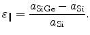
as  ) in the substrate. This can be seen in Fig. 2.2 where
the lattice structure of relaxed Si and Ge and strained Si on
SiGe is shown. The strain in the plane of the interface between the
strained layer and the substrate is given by the lattice mismatch,
) in the substrate. This can be seen in Fig. 2.2 where
the lattice structure of relaxed Si and Ge and strained Si on
SiGe is shown. The strain in the plane of the interface between the
strained layer and the substrate is given by the lattice mismatch,
 |
(2.1) |
Here,
 and
and
 denote the unstrained lattice constants
of Si and SiGe, respectively. Such a strain can only be sustained in thin
layers, and relaxation in the form of misfit dislocations will occur for thick
layers. An important criterion for growing strained Si layers without introducing
misfit dislocations is that the strained layer should have a thickness below
the critical value [Matthews74]. As a result of biaxial tensile strain,
carriers experience a lower resistance in the strained layer and typically have
50-70% higher mobilities [Nayak93,Welser92] in the channel direction.
denote the unstrained lattice constants
of Si and SiGe, respectively. Such a strain can only be sustained in thin
layers, and relaxation in the form of misfit dislocations will occur for thick
layers. An important criterion for growing strained Si layers without introducing
misfit dislocations is that the strained layer should have a thickness below
the critical value [Matthews74]. As a result of biaxial tensile strain,
carriers experience a lower resistance in the strained layer and typically have
50-70% higher mobilities [Nayak93,Welser92] in the channel direction.
Figure 2.2:
Lattice structure of (a) unstrained Si and SiGe. (b) strained
Si on relaxed SiGe.
Although most of the initial work on substrate-induced strain was limited by
increased defect densities and threading
dislocations [LeGoues92,Abstreiter85], sizable efforts were made to
tackle these problems through the usage of graded SiGe
buffers [Fitzgerald91] and chemical mechanical polishing
techniques [Currie98]. In order to further improve device performance,
it was a natural choice for the semiconductor industry to synergize the
mobility enhancement of strained Si with the low power benefits of SOI
technology.
The first kind of SOI based strained Si devices were fabricated by growing a
SiGe layer on top of an oxide layer. A SiGe layer was formed on the
oxide-capped Si substrate using different techniques such as
separation-by-implanted-oxygen (SIMOX), wafer bonding and layer transfer
techniques [Huang01,Sugiyama00], after which a strained Si layer was
grown on top of the SiGe layer. The technology thus matured with the name SGOI
(strained Si on relaxed SiGe on insulator). Due to the isolation provided by
the oxide layer, the junction capacitances are reduced while strained Si
results in higher mobilities, thereby increasing the overall performance. Ring
oscillator circuits utilizing the SGOI technology delivering 63% drain current
enhancement were reported [Mizuno03].
Although the two flavors of strained Si using SiGe, namely Si on
SiGe and SGOI, increase the device performance, there are several issues
due to the presence of Ge, which inhibit large scale integration. Firstly,
due to the different diffusion rate of dopants (B, As) in SiGe, the source and
drain extensions in these devices may cause increased short channel effects or junction
resistance problems. The diffusion of Ge into the strained Si layer poses
additional problems. Another major problem is the lower thermal conductivity of
SiGe which causes considerable self-heating of the devices [Jenkins02].
Therefore, a second kind of SOI-based devices followed wherein the SiGe buffer
layer was used only for generating strain in the Si layer but was later
eliminated from the final structure. Several techniques were
suggested [Rim03,Aberg04,Currie03] to bond a strained Si layer
directly onto an oxide-covered Si substrate, thus forming an SSDOI
(strained Si directly on insulator) device. This approach circumvents the
problems associated with SiGe and opens a new front for strain-based ultra thin
body and double gate devices. A schematic of the three types of strained
devices utilizing a SiGe substrate, is shown in Fig. 2.3.
Despite all the progress made in strained Si technology utilizing a SiGe
substrate, experimental observations suggested that this approach was probably
not the best choice for introducing strain into the channel. Biaxial strain was
found to give a higher mobility enhancement for electrons than for holes. Since
CMOS circuits already have a large area for the pMOS devices due to the poor
hole mobility, efforts to further enhance the electron mobilities could even
worsen the integration densities. Furthermore, biaxial strain can cause a
severe threshold voltage shift [Lim04], which also would significantly
bring down the device performance.
![\includegraphics[width=1.9in,angle=0]{figures/SSionSiGe.eps}](img111.png)
![\includegraphics[width=1.9in,angle=0]{figures/SGOI.eps}](img112.png)
![\includegraphics[width=1.9in,angle=0]{figures/SDOI2.eps}](img113.png)
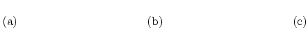
Figure 2.3:
Schematic of the three different types of strained Si technologies
utilizing a SiGe substrate. (a) Strained Si on SiGe, (b) SGOI and (c)
SSDOI.
Next: 2.2 Process-Induced Strain
Up: 2. Strained Si Technology
Previous: 2. Strained Si Technology
S. Dhar: Analytical Mobility Modeling for Strained Silicon-Based Devices
![\includegraphics[width=9.0in,angle=0]{figures/mod_Si_SiGe_lattice.eps}](img110.png)