


Next: 4.2 Modeling Approaches
Up: 4. Mobility Modeling
Previous: 4. Mobility Modeling
Subsections
4.1 Semiconductor Device Equations
The necessary equations which are solved in a numerical device simulator can be
obtained from Maxwell's equations and Boltzmann's transport equation.
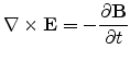
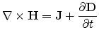
In differential and integral form, Maxwell's equations read
 |
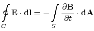 |
Faraday's Law of Induction |
 |
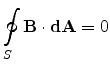 |
Gauss's Law of Magnetism |
 |
 |
Ampere's Circuital Law |
 |
 |
Gauss's Law of Electrostatics |
Here,
 denotes the magnetic field and
 the magnetic flux
density vector, while
the magnetic flux
density vector, while
 corresponds to the electric field and
 to the electric displacement vector. They are related through the
equations
to the electric displacement vector. They are related through the
equations
where the  and
and
 denote the relative magnetic permeability
and the relative dielectric permittivity of the medium, respectively.
denote the relative magnetic permeability
and the relative dielectric permittivity of the medium, respectively.
The wavelength associated with an operating frequency of say,  GHz, is
given by
GHz, is
given by
 |
(4.3) |
Since  is much greater than the typical device dimensions, which are
of the order of
is much greater than the typical device dimensions, which are
of the order of  , a quasi-stationary condition can be assumed for
the electric field which can be expressed as a gradient of a scalar potential
field,
, a quasi-stationary condition can be assumed for
the electric field which can be expressed as a gradient of a scalar potential
field,
 |
(4.4) |
Using (4.1) and (4.4) and Gauss's Law of Electrostatics, we
obtain Poisson's equation,
 |
(4.5) |
The space charge density  in semiconductors comprises of the mobile
charges and the fixed charges. Electrons and holes contribute to the mobile
charges while fixed charges are the ionized donors and acceptors,
in semiconductors comprises of the mobile
charges and the fixed charges. Electrons and holes contribute to the mobile
charges while fixed charges are the ionized donors and acceptors,
 |
(4.6) |
The  and
and  denote the electron and hole concentrations and
  corresponds
to the net doping concentration.
corresponds
to the net doping concentration.
Taking the divergence of Ampere's Circuital Law gives
 |
(4.7) |
The current density
 in semiconductors is the sum of the electron and
hole current densities denoted by
in semiconductors is the sum of the electron and
hole current densities denoted by
 and
and
 .
.
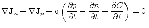 |
(4.8) |
Considering the fixed charges to be time-invariant
 , we get
The quantity  gives the net recombination rate for electrons and holes. A
positive value means recombination, a negative value generation of
carriers. Equations (4.9) and (4.10) are collectively known as
the carrier continuity equations.
gives the net recombination rate for electrons and holes. A
positive value means recombination, a negative value generation of
carriers. Equations (4.9) and (4.10) are collectively known as
the carrier continuity equations.
4.1.2 Transport Equations and Mobility
Prediction of the I-V characteristics of semiconductor devices requires precise
modeling of the mobility. A first principles calculation of mobility begins by
describing the state of the electron gas in microscopic terms, followed by set
of simplifying assumptions to arrive at macroscopic parameters that can
describe the state of the gas collectively. A widely used approach for
calculating mobility relies on the Boltzmann transport equation (BTE) which is
an integro-differential equation based on both statistical and classical laws
of dynamics.
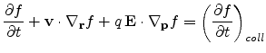 |
(4.11) |
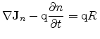
Figure 4.1:
Classification of different scattering mechanisms in Si adapted
from [Lundstrom00].
Here
 denotes the single particle
distribution function,
denotes the single particle
distribution function,
 denotes the group velocity of electrons and
is the applied electric field. The left hand term in (4.11)
describes the evolution of the distribution function with time in the six
dimensional phase space of coordinates
denotes the group velocity of electrons and
is the applied electric field. The left hand term in (4.11)
describes the evolution of the distribution function with time in the six
dimensional phase space of coordinates
 and
and
 in the
presence of externally applied forces. The right hand side term corresponds to
the effect of various scattering mechanisms on the distribution function.
in the
presence of externally applied forces. The right hand side term corresponds to
the effect of various scattering mechanisms on the distribution function.
Electrons and holes are accelerated by the electric field, but lose momentum as
a result of various scattering processes. These scattering mechanisms
contributing to the collision term in (4.11) are due to lattice vibrations
(phonons), impurity ions, other carriers, surfaces, and other material
imperfections. Fig. 4.1 shows a chart describing the various
mechanisms of carrier scattering in a semiconductor. The effects of all of
these microscopic phenomena are lumped into the macroscopic mobility introduced
by the transport equation. However, in its original form, the BTE does not
yield a closed form solution for mobility, and only after making certain
assumptions, such as the relaxation time approximation, can the solutions be
worked out. The resulting mobility can be expressed as
 |
(4.12) |
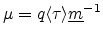
where
 denotes the average momentum relaxation time and
 is the effective mass tensor. The mobility expression
in (4.12) is popularly referred to as the Drude
model [Drude00]. It is apparent that the value of
directly affects the value of the mobility, and thus characterization of
scattering mechanisms helps in estimating the mobility. For Si and Ge, the
effective mass tensor is diagonal with equal diagonal components and therefore
the mobility can be expressed as a scalar,
is the effective mass tensor. The mobility expression
in (4.12) is popularly referred to as the Drude
model [Drude00]. It is apparent that the value of
directly affects the value of the mobility, and thus characterization of
scattering mechanisms helps in estimating the mobility. For Si and Ge, the
effective mass tensor is diagonal with equal diagonal components and therefore
the mobility can be expressed as a scalar,  .
.
In an actual sample of Si, multiple mechanisms can act to scatter the
motion of electrons. Based on the assumption of the statistical independence of the scattering
mechanisms, the scattering rates may be added using Matthiessen's
rule [Nishida87]
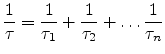 |
(4.13) |
where independent scattering mechanisms are involved. The overall mobility
is therefore given by
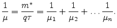 |
(4.14) |
Transport in semiconductors can occur through the application of an electric
field or through a gradient of carrier concentrations, temperature or material
properties. Taking into consideration the effect of electric field and
concentration gradients, an expression for the current density can be obtained
from the Boltzmann's transport equation, as shown below.
Making use of the relaxation time approximation (RTA), the collision term on
the RHS of (4.11) can be replaced by
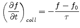 |
(4.15) |
where  denotes the equilibrium distribution function. Assuming steady
state conditions, the one-dimensional BTE can now be written as
denotes the equilibrium distribution function. Assuming steady
state conditions, the one-dimensional BTE can now be written as
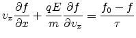 |
(4.16) |
Multiplying (4.16) with  and integrating over the
three-dimensional velocity space gives
and integrating over the
three-dimensional velocity space gives
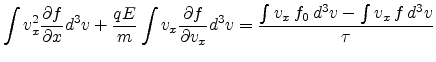 |
(4.17) |
Since the equilibrium function is symmetric, the first integral on the RHS
in (4.17) vanishes, and the RHS of (4.17) becomes
 |
(4.18) |
and therefore, we have,
 |
(4.19) |
Evaluating the integrals in (4.19),
Introducing the mobility as in (4.12) and the average value
 as
as
 , the current density
in (4.19) becomes
, the current density
in (4.19) becomes
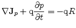
A similar equation is obtained for the hole current density.
The Poisson equation (4.5) together with the continuity
equations (4.9) and (4.10) and the current density
relations (4.22) and (4.23) constitute the fundamental equations
for performing drift diffusion based simulations.
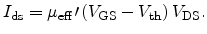
The drain current of an MOS transistor as a function of the gate and drain
biases can be computed from the Poisson's equation by making the gradual
channel approximation and the charge sheet approximation, as described
in [Taur98].
![$\displaystyle \hspace*{-0cm} \ensuremath{I_\mathrm{ds}}= \mu_\ensuremath{{\math...
...V_\mathrm{DS}}}{2\ensuremath{\Phi_\mathrm{B}}}\right)^{3/2} - 1 \right] \right]$](img461.png) |
(4.24) |
Here,
 , with
 as the carrier
mobility and
as the carrier
mobility and  as the device width and
  as the gate length.
In the linear regime, where
as the gate length.
In the linear regime, where
 |
(4.25) |
the drain current expression can be simplified to
 |
(4.26) |
In the saturation regime, where
 |
(4.27) |
the drain current is modeled as
![$\displaystyle \ensuremath{I_\mathrm{ds}}= \mu_\ensuremath{{\mathrm{eff}}}\prime...
...{DS}}- m\ensuremath{V_\mathrm{DS}}^2] (1 + \lambda \ensuremath{V_\mathrm{DS}}),$](img467.png) |
(4.28) |
where denotes the channel length modulation parameter. The quantity
 denotes the threshold voltage and is obtained as
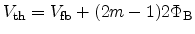 |
(4.29) |
Here
 is the flat band voltage
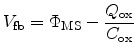 |
(4.30) |
and  is the body-effect coefficient defined as
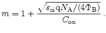 |
(4.31) |
The potential
 is evaluated as
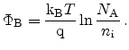 |
(4.32) |
In (4.31),
 is the permittivity of the Si
substrate,
is the permittivity of the Si
substrate,
 the acceptor doping concentration, and
 the
capacitance per unit area of the oxide. The
the
capacitance per unit area of the oxide. The  denotes the intrinsic carrier
concentration of Si,
denotes the intrinsic carrier
concentration of Si,
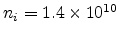 cm
cm at 300 K.
From equations (4.26) and (4.28) it is seen that the drain
current is directly proportional to the mobility
. Therefore,
employment of strained Si, which enhances the mobility, results in an increase
in the drain current, thereby making circuits faster. Moreover, since strain
causes a relative shift of the conduction and valence band minima, it can
result in a reduced threshold voltage due to a decreased work function
difference
 .
.
Next: 4.2 Modeling Approaches
Up: 4. Mobility Modeling
Previous: 4. Mobility Modeling
S. Dhar: Analytical Mobility Modeling for Strained Silicon-Based Devices
![$\displaystyle \int{dv_y} \int{d v_z} \int{v_x \frac{\partial f}{\partial v_x}dv_x} = \int{dv_y} \int{d v_z} [v_x f]_{-\infty}^{\infty} - \int{f d^3v} = -n$](img455.png)
![\includegraphics[width=6.0in,angle=0]{figures/FlowScattering.eps}](img437.png)
![$\displaystyle {\mathbf{J}}_n = q \mu_n \left [ n {\mathbf{E}} + \frac{kT}{q} \ensuremath{{\mathbf{\nabla}}}n\right].$](img459.png)
![$\displaystyle {\mathbf{J}}_p = q \mu_p \left [ p {\mathbf{E}} - \frac{kT}{q} \ensuremath{{\mathbf{\nabla}}}p \right]$](img460.png)