The equivalent circuit is plotted in
Fig. 7.5. The operating principle is based on moving the
charge between the bit line capacitor ![]() and the
ferroelectric capacitor
and the
ferroelectric capacitor ![]() . The drawback of this
method is that an external reference voltage has to be generated in
order to allow the evaluation of the memory state.
. The drawback of this
method is that an external reference voltage has to be generated in
order to allow the evaluation of the memory state.
During write operation, the memory cell is accessed by raising the
wordline (WL) voltage, which turns the access transistor in ON state,
and at the same time pushes the ferroelectric capacitor into negative
saturation, no matter whether the cell was in the ``1'' or ``0''
state. In the second half of the write cycle, the plateline (PL)
voltage is raised. As the transistor is in the ON state, the
potential difference between bitline (BL) and plateline modifies the
operating point of the capacitor. In case of ``0'', the bitline is not
raised and ![]() will be in positive saturation, and after
the write cycle is finished,
will be in positive saturation, and after
the write cycle is finished, ![]() will be defined by the
positive remanent polarization
will be defined by the
positive remanent polarization
![]() . If the bitline is
raised and a ``1'' is written, the potential difference will be
insignificantly low and
. If the bitline is
raised and a ``1'' is written, the potential difference will be
insignificantly low and ![]() will be at the negative
remanent polarization
will be at the negative
remanent polarization
![]() , and remain there after the
write cycle.
, and remain there after the
write cycle.
Fig. 7.8 shows the timing diagram of the read cycle.
At first the bitline is actively set to 0V. After the bitline
capacitor is discharged, writeline and plateline are activated using
the supply voltage ![]() . Now
. Now ![]() and
and ![]() form a capacitive
voltage divider between plateline and ground. Depending on the
information in the memory cell, the operating points of the
ferroelectric material differ, and so does the capacity of
form a capacitive
voltage divider between plateline and ground. Depending on the
information in the memory cell, the operating points of the
ferroelectric material differ, and so does the capacity of ![]() . If
the ferroelectric hysteresis is approximated by two different
capacitors (Fig. 7.7), the bitline voltage reads as
. If
the ferroelectric hysteresis is approximated by two different
capacitors (Fig. 7.7), the bitline voltage reads as
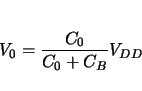 |
(7.1) |
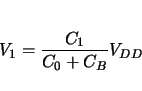 |
(7.2) |
if the stored information is ``1''. These two different voltages are detected by the sense amplifier, and, similarly to the 2C2T structure, the original information is restored in the memory cell.
![\resizebox{\fulllength}{!}{
\psfrag{Bit Line}{Bitline}
\psfrag{Plate Line}{Plate...
...V_{C_\mathrm{B}}$}
\includegraphics[width=\fulllength]{figs/1T1C_curcuit.eps}
}](img351.gif)
![\resizebox{\halflength}{!}{
\psfrag{BL}{BL}
\psfrag{WL}{WL}
\psfrag{PL}{PL}
\psf...
...'}
\psfrag{1}{\lq\lq 1''}
\includegraphics[width=\halflength]{figs/sense_1C1T.eps}
}](img355.gif)
![\resizebox{\halflength}{!}{
\psfrag{C1}{$C_1$}
\psfrag{C0}{$C_0$}
\includegraphics[width=\halflength]{figs/approx.eps}
}](img356.gif)
![\resizebox{\halflength}{!}{
\psfrag{BL}{BL}
\psfrag{WL}{WL}
\psfrag{PL}{PL}
\psf...
...sfrag{1}{\lq\lq 1''}
\includegraphics[width=\halflength]{figs/sense_1C1T_read.eps}
}](img357.gif)