6.2 Drive-current enhancement
The application of electrostatic lenses to focus electrons can be used to increase the performance of actual devices. This novel concept is presented here (based on
[156]).
The dimensions of the channel in modern transistor architectures, like multigate-FETs or UTB-SOI, have progressively been scaled down to retain adequate
electrostatic control of the channel. The connecting source/drain extensions, however, remain relatively large and have started to play a significant role in the overall
performance of the device [157]. Therefore, considerations are made to optimize these regions, e.g. to reduce the contact and access resistances [158, 159]. An
electrostatic lens in the source region can be used to increase the drive-current through the channel by focusing the electrons into the channel aperture and thereby
reducing reflections from the adjacent oxide.
6.2.1 Geometry
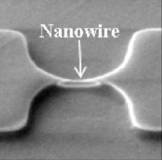
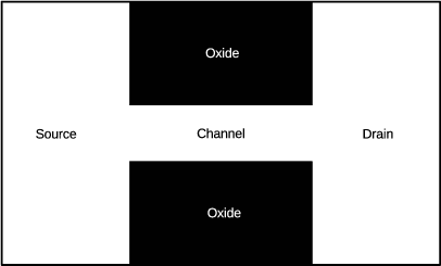
A geometry representative for many current transistor structures in which a narrow channel  is surrounded/sandwiched by oxide and is extended to a larger
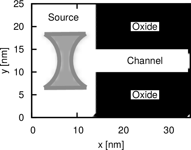
drain/source contact region is shown in Figure 6.8. The geometry considered for the simulations is shown in Figure 6.9 omits the drain region. The oxide is
approximated by a 0.4eV barrier, which is sufficient to constrain the wavepackets to the channel and source regions without inducing excessive particle generation
(the generation rate is related to the magnitude of the potential differences).
is surrounded/sandwiched by oxide and is extended to a larger
drain/source contact region is shown in Figure 6.8. The geometry considered for the simulations is shown in Figure 6.9 omits the drain region. The oxide is
approximated by a 0.4eV barrier, which is sufficient to constrain the wavepackets to the channel and source regions without inducing excessive particle generation
(the generation rate is related to the magnitude of the potential differences).
Wavepackets are periodically injected from the left boundary towards the channel (discussed further hereafter). A converging electrostatic lens is placed before the
aperture of the channel to focus the wavepackets into the channel. The De Broglie wavelength of the wavepackets considered here is in the order of a few nanometres,
which requires the lens to be at least 10nm wide to avoid diffraction effects.
6.2.2 Steady-state current
The feasibility of investigating time-resolved quantum transport presents one of the biggest advantages of Wigner formalism based simulations. However, the
steady-state behaviour of devices is of considerable importance in many applications. The possibility to obtain a steady-state solution is also of interest to be able to
strike a comparison with the results obtained by the NEGF approach. The approach presented here to calculate the current is intended to make a qualitative
investigation possible. A validation of this approach was done by counting the charge crossing the absorbing boundaries (the left source and the right drain) over a
time interval.
In order to calculate the steady-state current in a device, minimum uncertainty wavepackets (3.34) are periodically injected from the left boundary representing the
source contact. Here, identical wavepackets, with the parameters defined in Table 6.1 with a mean energy of approximately 200meV are injected. A distribution
function, e.g. Maxwell-Boltzmann shaped, can also be sampled to select the mean energy (wavevector) of each individual wavepacket injected from the source
contact.
Table 6.1: Simulation parameters for injected wavepackets and domain
| r0 [nm] | σ [nm] | Lcoh [nm] | k0 [nm-1] | Δx [nm] |
 | 3/5 | 30 |  | 0.5 |
| |
The drive-current (through the channel) is calculated by the Ramo-Shockley theorem [161], adapted to account for the signed numerical particles used in the WMC
simulator:
where Lx, Nwp and e represent the device length in the x-direction (35nm), the number of numerical particles representing one injected wavepacket and the unit
charge, respectively. The summation is performed over all particles in the device, taking the sign (si) and the x-velocity (vi) of each numerical particle into account.
The electric field is assumed to be uniform across the channel, directed rightwards, i.e. E = (0,Ex).
Since each wavepacket represents a single electron, the magnitude of the injected current can be set by the period of injection Tinj, i.e.
6.2.3 Results
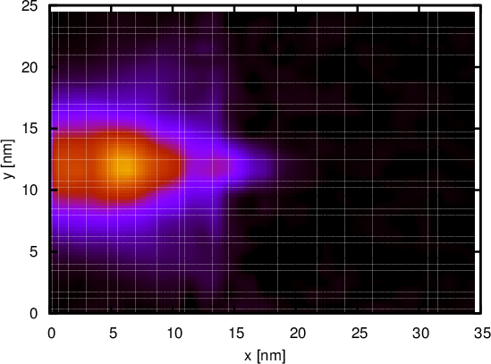
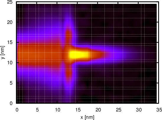
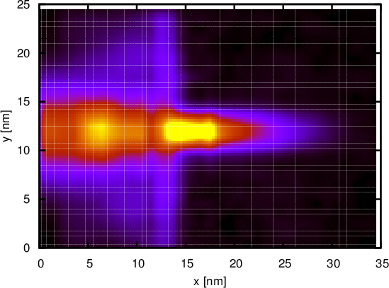
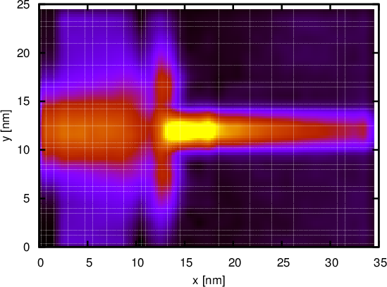
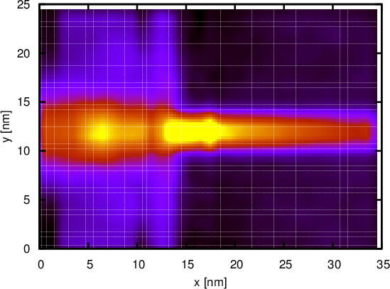
Simulations, using the geometry in Figure 6.9, are run with and without the addition of a converging lens in front of the aperture to the channel.
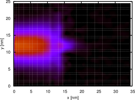
Figure 6.10 compares the evolution of the probability density towards a steady state with and without a lens. Without the lens a large portion of
the wavepacket is reflected from the oxide adjacent to the aperture of the channel, thereby reducing the drive-current. With the addition of a
converging lens, the wavepackets can be focused to move into the channel, thereby reducing the reflections from the oxide barriers next to the
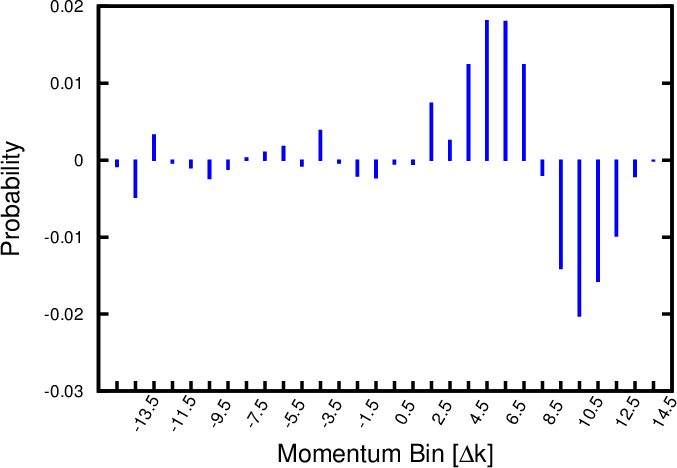
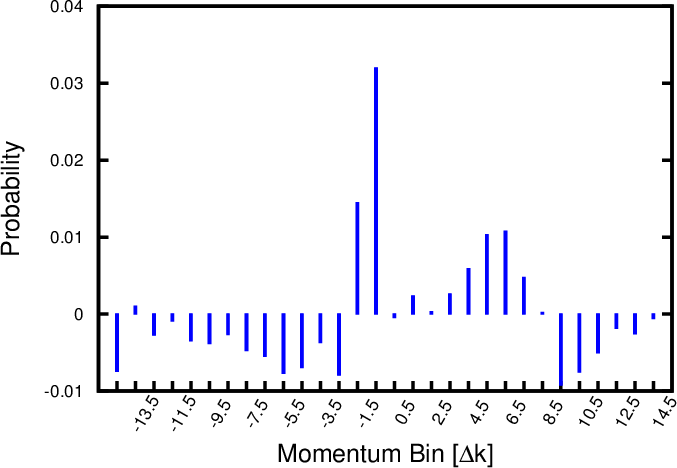
aperture of the channel. This observation is supported by the associated difference of the kx-distributions. Figure 6.11 (a) shows the change in
kx-distributions corresponding to Figure 6.10 (a); the reduction in the kinetic energy of the wavepackets due to the barrier presented by the
lens is clearly shown. However, once the steady-state is reached (at approximately t = 140fs; Figure 6.11 (b)) a reduction in the probability of
left-moving (negative kx) particles is observed, indicating the lens leads to reduced reflections overall; the forward-moving particles (around 5Δk) are
enhanced.
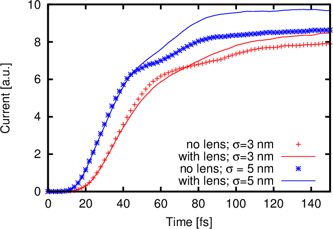
The steady-state current is calculated for wavepackets with a standard deviation of 3nm and 5nm, as shown in Figure 6.12. The addition of the lens consistently
increases the drive current; the gains made by focusing the wavepackets into the channel are larger than the losses from reflections by the lens, which presents a small
barrier to the electrons. The lens shows a better effect, when a (spatially) broader wavepacket is focused and increases the channel current by 15% if σ = 5nm,
compared to an 8% increase if σ = 3nm. Some uncertainty exists about the true value of the standard deviation for the wavepacket [34]. Moreover, the Gaussian
wavepacket spreads out as it propagates. The current gradually rises as the domain is filled with particles before it converges to a steady-state value after
approximately 140fs.
It is concluded that the addition of a converging electrostatic lens in the source region of a transistor can be used to effectively focus electron wavepackets into a
nanoscale channel by reducing reflections from the oxide surrounding the aperture. Moreover, the results illustrate for the first time how a
steady-state current is obtained with a two-dimensional WEMC simulator, allowing it to be applied to investigate practical issues of semiconductor
devices.