


Next: 3. The Silicon/Silicon-Dioxide Interface
Up: 2. Simulation of Semiconductor
Previous: 2.3 Carrier Generation and
Subsections
The classical semiconductor device equations from Section 2.1
imply that the mobile carriers, electrons and holes, behave like classical
particles in the semiconductor. For large device dimensions this assumption
gives very good results, but for small device geometries quantum mechanical
effects like the quantum mechanical tunneling, described in Section 5.3,
and the quantum mechanical confinement gain importance. The latter effect
leads to a reduction of allowed states for electrons and holes near a
 interface. In classical device simulations using the drift-diffusion
approximation the peak of the electron concentration in the channel of a turned
on n-channel MOSFET is calculated to be directly at the
interface.
This is not correct as the number of allowed states is drastically reduced
close to the interface and therefore the peak of the carrier concentration lies
several angstroms away from the interface [9].
interface. In classical device simulations using the drift-diffusion
approximation the peak of the electron concentration in the channel of a turned
on n-channel MOSFET is calculated to be directly at the
interface.
This is not correct as the number of allowed states is drastically reduced
close to the interface and therefore the peak of the carrier concentration lies
several angstroms away from the interface [9].
2.4.1 Quantum Confinement
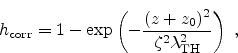
For the modeling of NBTI the carrier concentration close to the
interface plays an important role (Section 6.4.4). The use
of quantum confinement models reduces this carrier concentration and might have
significant influence on the NBTI model used.
In classical device simulators quantum confinement is often accounted for by
using additional quantum correction models. These models locally change the
carrier density-of-states [10,11] or they modify the
conduction band edge close to the interface [12].
In classical device simulation the density-of-states (DOS) in homogeneous
materials is modeled as a constant value throughout the device. In order to
describe the quantum mechanical confinement a distance-dependent reduction of
the DOS at the
interface has been proposed
in [10,11]
 |
(2.106) |
where  is the distance to the
interface and
is the distance to the
interface and  shifts the whole
function relative to the interface.
shifts the whole
function relative to the interface.  is a newly introduced parameter
which enables the variation of
is a newly introduced parameter
which enables the variation of
 for calibration
purposes. The symbol
denotes the thermal wavelength which
is given by
for calibration
purposes. The symbol
denotes the thermal wavelength which
is given by
 |
(2.107) |
where  is the reduced Planck constant,
  is the effective carrier
mass,
is the effective carrier
mass,
 the Boltzmann constant, and
  the temperature. The resulting
DOS,
the temperature. The resulting
DOS,  , is then calculated from the classical DOS
 , which is normally modeled as a constant throughout the
semiconductor, with the correction factor
, which is normally modeled as a constant throughout the
semiconductor, with the correction factor
 as
as
 |
(2.108) |
Figure 2.5:
Plot of the DOS correction factor
 for
for  nm
and
nm
and  at
at  K.
K.
|
|
The interplay of the different parameters and the distance to the
interface is schematically depicted in Figure 2.5. The parameter
is important, because with  the DOS at the interface becomes zero.
This would cause numerical problems and reduce the convergence of the numerical
solver. A positive number of shifts the correction function towards the
dielectric, approximately considering wave function penetration. The value of
the DOS at the interface becomes zero.
This would cause numerical problems and reduce the convergence of the numerical
solver. A positive number of shifts the correction function towards the
dielectric, approximately considering wave function penetration. The value of
 defines the effective depth of the correction. A
high value, which can be achieved with
defines the effective depth of the correction. A
high value, which can be achieved with  , leads to a reduction of the
DOS even deep in the substrate.
, leads to a reduction of the
DOS even deep in the substrate.
Note that the correction factor does not depend on the bias and the band edge
energies are not influenced. Hence, the model can be evaluated in a
preprocessing step and does not impose any additional computational burden
during iteration steps.
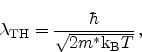
Figure 2.6:
Band edge bending at the
interface. The classical band edge
is corrected by the factor
 .
.
|
|
An alternative approach is based on  , the first eigenvalue of the
triangular energy well, as seen in Figure 2.6. This model was proposed by
van Dort [12]
, the first eigenvalue of the
triangular energy well, as seen in Figure 2.6. This model was proposed by
van Dort [12]
 |
(2.109) |
where the proportionality factor
 is
is found from the observed threshold voltage shift at high doping
levels [13],
is
is found from the observed threshold voltage shift at high doping
levels [13],
 is the permittivity of
silicon, and
is the permittivity of
silicon, and  is the electric field at the
interface
perpendicular to the interface.
is the electric field at the
interface
perpendicular to the interface.
The value of
 is multiplied with a distance-dependent
weight function which has been introduced by Selberherr [14] for
the modeling of surface roughness scattering in MOSFETs. The function is of the
following form
is multiplied with a distance-dependent
weight function which has been introduced by Selberherr [14] for
the modeling of surface roughness scattering in MOSFETs. The function is of the
following form
 |
(2.110) |
where
 is the scaling factor for the interface distance. Thus,
the resulting band edge energy with van Dort's quantum correction of the
classical band edge energy
is the scaling factor for the interface distance. Thus,
the resulting band edge energy with van Dort's quantum correction of the
classical band edge energy
 reads as follows
 |
(2.111) |
Figure 2.6 depicts the distance dependent weight function  and the band
edge energy for both, the classical approach and after quantum correction with
van Dort's method.
and the band
edge energy for both, the classical approach and after quantum correction with
van Dort's method.
For the evaluation of the quantum correction models a state-of-the-art
three-dimensional n-channel FinFET device structure was chosen. The device
geometry can be seen in Figure 2.7.
Figure 2.7:
Device geometry of a triple-gate FinFET structure. Quantum
confinement plays an important role in this device because of its small size
and the formation of three, instead of one, channels.
|
|
The silicon fin has a cross section area of 6 10nm
10nm . The gate
length is 20nm with a gate oxide thickness of 1.5nm. The source and drain
regions are heavily n-type doped whereas the channel itself remains undoped.
. The gate
length is 20nm with a gate oxide thickness of 1.5nm. The source and drain
regions are heavily n-type doped whereas the channel itself remains undoped.
Figure 2.8:
Electron concentration in a triple-gate FinFET for classical
simulation (left), with the DOS correction model (middle), and the band edge
energy correction model by Van Dort. The correction models force the peak of
the carrier concentration away from the
interface into the
substrate.
|
|
Figure 2.8 depicts the electron concentration in a two-dimensional cut
through the silicon fin in the middle of the channels. The gates are biased at
0.9V with the source and drain contacts grounded. The classical simulation
using the drift-diffusion approximation gives the highest magnitude of the
electron concentration at the
interfaces below the gate contacts. It
can be seen that the peak electron concentration is found in the top corners,
as two respective gates couple to the channel, each of them attracting
carriers. With the quantum confinement correction models the maximum carrier
concentration is moved to the inside of the fin by a distance depending on the
chosen model and its calibration parameters.
Figure 2.9:
Electron concentration across the fin using classical device
simulation and the confinement correction models.
|
|
Figure 2.9 depicts a one-dimensional cut through the fin displaying the
carrier concentrations for the different models for the same bias conditions.
Comparing with Figure 2.10 reveals that qualitatively the DOS correction
model delivers better results.
Figure 2.10:
Comparison of classical and quantum mechanical carrier
concentrations for different fin widths. The quantum mechanical calculations
have been performed using a Schrödinger solver.
|
|
A comparison of FinFETs with different fin widths can be seen in
Figure 2.10. It shows the electron concentration across the fin
simulated with both, the classical drift-diffusion model and a Schrödinger
solver, respectively. The fin widths are 6, 12, and 18nm. At a fin width of
6nm the electron concentration has its maximum in the center of the fin. This
shape of the carrier concentration cannot be reproduced by the quantum
correction models. With larger widths the maximum moves to the interfaces
enabling a better fit of the correction models.
Figure 2.11:
Comparison of the output characteristics of double- and triple-gate
FinFETs at a gate voltage of 0.9 V. Quantum confinement correction
reduces the drain current as no carriers are allowed at the
interface.
|
|
The channels in the silicon fin are displaced from the surface to the inside of
the silicon and thus the drive current is reduced. Figure 2.11 depicts
the drain current for a gate voltage of 0.9V and different quantum correction
mechanisms. Additionally to the triple-gate device the simulation has been
performed with a double-gate structure, where the top gate from Figure 2.7
has been replaced with
 . Simulation of the double-gate structure shows a
reduced output current by a factor of approximately 20% due to the formation
of only two channels.
. Simulation of the double-gate structure shows a
reduced output current by a factor of approximately 20% due to the formation
of only two channels.
Quantum correction leads to a considerable reduction of the saturation current.
The DOS correction model yields reasonable results, but since it does not
account for the band bending it must be calibrated for each bias point. Van
Dort's model completely fails to reproduce the carrier concentration in the
channel which may be due to the assumption of a triangular energy well. This
assumption might be a too crude estimation for extremely thin channels.
Therefore, these models can be very well used to describe the current reduction
in very thin channel devices, but not when the shape of the carrier
concentration is important. Here, the solution of Schrödinger's equation is
necessary for accurate simulation of the carrier concentration.
Next: 3. The Silicon/Silicon-Dioxide Interface
Up: 2. Simulation of Semiconductor
Previous: 2.3 Carrier Generation and
R. Entner: Modeling and Simulation of Negative Bias Temperature Instability
![\includegraphics[width=10cm]{figures/vandort}](img300.png)
![\includegraphics[width=10cm]{figures/finfet}](img312.png)
![\includegraphics[width=16cm]{figures/cut-econcentrations}](img315.png)
![\includegraphics[width=\figwidth]{figures/econc_rot}](img316.png)
![\includegraphics[width=\figwidth]{figures/qmclassic_rot}](img317.png)
![\includegraphics[width=\figwidth]{figures/outputchar-color}](img318.png)
![\includegraphics[width=\figwidth]{figures/haenschcorr-new}](img296.png)