The charge-pumping effect in MOS devices has been reported
by J.S.Brugler and P.G.A.Jespers in 1969 [43] and by A.Goetzberger and
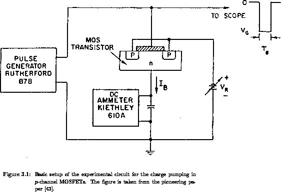
E.H.Nicollian in [148] for the first time . They have
measured a DC component of the bulk current when periodic voltage pulses are
applied to the gate in the circuit shown in Figure 3.1. This
current was in the opposite direction and much larger than the leakage current
of the reversely biased source and drain junctions. It was proportional to the
pulse frequency and the gate area. This current is called the charge-pumping
current
. They have
measured a DC component of the bulk current when periodic voltage pulses are
applied to the gate in the circuit shown in Figure 3.1. This
current was in the opposite direction and much larger than the leakage current
of the reversely biased source and drain junctions. It was proportional to the
pulse frequency and the gate area. This current is called the charge-pumping
current  . In the pioneering work [43] the authors have given
a correct qualitative physical explanation of the effect.
. In the pioneering work [43] the authors have given
a correct qualitative physical explanation of the effect.
Neglecting the junction leakage current, the DC component of the bulk current
is caused by two effects (for  -channel MOSFETs):
The first effect has been extensively used in the last ten years to extract the
amount and the distribution (in both, energy and position space) of traps
in MOS devices. In these measurements, the second effect introduces a parasitic
undesired component which can be removed in most cases. The reasons for
an increasing popularity of charge pumping are its simplicity, high
sensitivity, good accuracy and its direct applicability on small devices.
Charge pumping is mostly applied to analyze the localized degradation after
hot-carrier stress in
MOSFETs [423][374][288][287][196][194][34][9].
Its ability to be performed on small devices (with real design dimensions)
is particularly useful in studying the nonuniform degradation of memory
MOS devices (EPROMs and EEPROMs) under working
conditions [510][509][214][196]. Uniform degradation caused by
E-beam [196] and  -rays [495] irradiation and by
Fowler-Nordheim injection [495][196][76] has been studied by the
charge pumping as well. A particular problem is to study traps in SOI devices,
where both, front and back interface play an important role in determining
the properties of those devices. Detailed studies are presented in [515]
for laser-recrystallized silicon films, in [445] for epitaxial films
and in [357][116] for the SIMOX
technology. A specific application is to evaluate the traps at grain boundaries
in polysilicon-film devices [258][257]. In this case the measured
quantity (charge-pumping current) contains a direct information on the traps at
grain boundaries. Note that in the conventional current-related techniques to
study the polysilicon devices, the device current is affected by the barriers
at the grain boundaries, while the barriers are influenced by the traps at
grain boundaries, as well as by the dopant concentration. Therefore, the
measured drain current contains an indirect information on the traps. The
extracted trap density is model-dependent in these cases.
-rays [495] irradiation and by
Fowler-Nordheim injection [495][196][76] has been studied by the
charge pumping as well. A particular problem is to study traps in SOI devices,
where both, front and back interface play an important role in determining
the properties of those devices. Detailed studies are presented in [515]
for laser-recrystallized silicon films, in [445] for epitaxial films
and in [357][116] for the SIMOX
technology. A specific application is to evaluate the traps at grain boundaries
in polysilicon-film devices [258][257]. In this case the measured
quantity (charge-pumping current) contains a direct information on the traps at
grain boundaries. Note that in the conventional current-related techniques to
study the polysilicon devices, the device current is affected by the barriers
at the grain boundaries, while the barriers are influenced by the traps at
grain boundaries, as well as by the dopant concentration. Therefore, the
measured drain current contains an indirect information on the traps. The
extracted trap density is model-dependent in these cases.
The second application of charge pumping is to employ it for device operation.
Much less attention has been paid to this type of application in the past (at
least in the literature). Some examples of the so-called charge-pumping devices
will be given henceforward. In the work [113] (1975) by an INTEL group,
the charge-pumping effect is used to refresh the storage gate capacitance in a
two-MOS-transistor bistable memory cell. Both effects, 1 and 2 described
above, can be involved at device operation. A 4096-bit memory array is
realized with these cells. Here, the feature that the charge-pumping effect
produces a DC current in the opposite direction to the junction-leakage current
(which discharges the node) is used. The charge-pumping current predominates
over the leakage currents and charges the corresponding gate capacitance in a
bistable configuration. The same feature is used in [53][50]
(and references therein) by U.Cilingiroglu, where charge pumping at the
node itself is applied to refresh the floating storage node. The difference
between the charge-pumping and the leakage current yields two stable
conditions at the  characteristics of the gated-diode. By adding a gate
resistor [53] or by capacitive coupling [50] the storage
node can exhibit bistability with a regenerative loop. A different type of
charge-pumping devices is proposed by N.Sasaki in [407][405]. During
charge pumping the minority carriers can be injected by effect 2 into the
bulk of SOI MOSFETs (SOS technology has been considered
in [407][405]). The injected charge remains in the floating substrate,
because the substrate potential (its absolute value) increases and reversely
biases the source and drain junctions. The increase of the bulk potential is
independent of the duration of the top and bottom levels, while it depends on
the fall time of the gate pulse (Figure 3.2). The presence of
the charge in the bulk can be detected as a change in device conductivity.
Using the avalanche effect the charge can be removed from the bulk. This
concept has been implemented in an one-device memory cell [407] which
has been applied to build a memory array [406].
characteristics of the gated-diode. By adding a gate
resistor [53] or by capacitive coupling [50] the storage
node can exhibit bistability with a regenerative loop. A different type of
charge-pumping devices is proposed by N.Sasaki in [407][405]. During
charge pumping the minority carriers can be injected by effect 2 into the
bulk of SOI MOSFETs (SOS technology has been considered
in [407][405]). The injected charge remains in the floating substrate,
because the substrate potential (its absolute value) increases and reversely
biases the source and drain junctions. The increase of the bulk potential is
independent of the duration of the top and bottom levels, while it depends on
the fall time of the gate pulse (Figure 3.2). The presence of
the charge in the bulk can be detected as a change in device conductivity.
Using the avalanche effect the charge can be removed from the bulk. This
concept has been implemented in an one-device memory cell [407] which
has been applied to build a memory array [406].