Before analyzing the degradation of  -channel lightly-doped drain (LDD)
MOSFETs by means of charge pumping it is important to understand the
charge-pumping characteristics of these devices before electrical stress
(virgin devices).
-channel lightly-doped drain (LDD)
MOSFETs by means of charge pumping it is important to understand the
charge-pumping characteristics of these devices before electrical stress
(virgin devices).
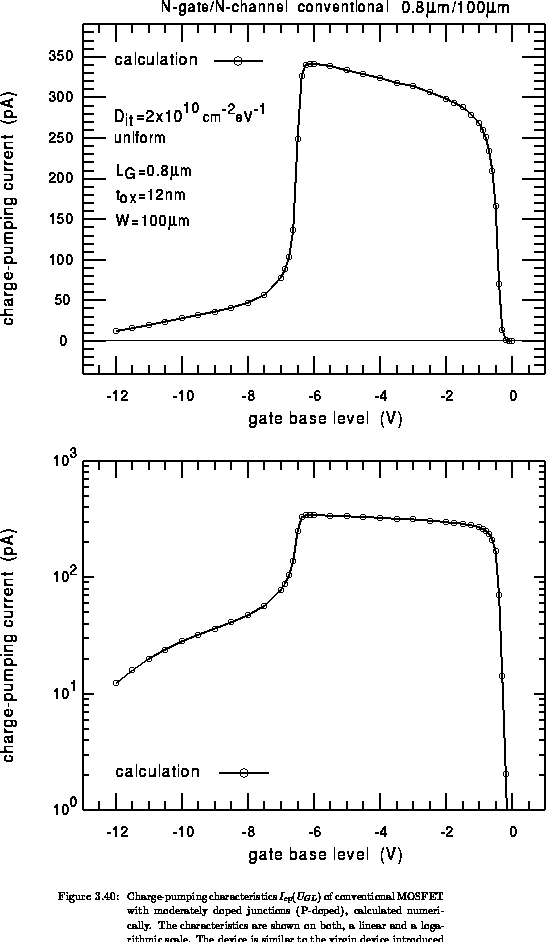
The charge-pumping characteristics of virgin LDD MOSFETs differ qualitatively
from the same characteristics of the conventional MOSFETs with abrupt source
and drain junctions. Figure 3.40 shows the charge-pumping
current versus the gate base level,  calculated numerically
for the conventional -channel MOSFET considered in
Appendix D and Section 3.5.2. The
characteristics are plotted on both, a linear and a logarithmic scale. The
device parameters are given in Appendix D. The corresponding
characteristics of an -channel LDD MOSFET with the same gate length
(
calculated numerically
for the conventional -channel MOSFET considered in
Appendix D and Section 3.5.2. The
characteristics are plotted on both, a linear and a logarithmic scale. The
device parameters are given in Appendix D. The corresponding
characteristics of an -channel LDD MOSFET with the same gate length
( ) are presented in
Figures 3.41 and 3.42. Both devices have a
similar geometry and the same interface-trap density. Apparently, there are two
characteristic tails at the rising edge of the curve for the LDD device compared
to one tail on the characteristics of the conventional MOSFET. The first short
tail for the LDD device is located just under the charge-pumping threshold
voltage of the channel region. The second tail extends from the end of the first
tail deeply towards the negative gate bias, like the tail of the conventional
device. Similar features are found on the characteristics reported in the
literature [384][196]. These qualitative differences are explained
below.
) are presented in
Figures 3.41 and 3.42. Both devices have a
similar geometry and the same interface-trap density. Apparently, there are two
characteristic tails at the rising edge of the curve for the LDD device compared
to one tail on the characteristics of the conventional MOSFET. The first short
tail for the LDD device is located just under the charge-pumping threshold
voltage of the channel region. The second tail extends from the end of the first
tail deeply towards the negative gate bias, like the tail of the conventional
device. Similar features are found on the characteristics reported in the
literature [384][196]. These qualitative differences are explained
below.
Let us discuss the charge-pumping characteristics of the conventional devices
at first. The characteristics of those devices exhibit one long tail, ranging
from a very negative gate bottom level to the charge-pumping threshold voltage
of the channel region. The slope of the curve at the channel charge-pumping
threshold is high. The slope of the falling edge of the characteristics
is very high, too. Three effects influence the slopes of the rising and
falling edges of the curve in conventional MOSFETs:
curve, respectively. This intrinsic charge-pumping effect
is slight. Considering MOSFETs, it becomes important when the third,
junction effect vanishes (discussed below), as is the case at the
steep rising part, close to the channel threshold and at the falling
edge of the characteristics. A detailed analytical investigation of this
effect is introduced in Section 3.3.
, because the trapped charge
effectively shifts the charge-pumping threshold and flat-band voltage.
This effect is significant for high trap densities only. The trapped
charge depends directly on the surface carrier concentration, while
the latter depends exponentially on the surface potential,
i.e. on the gate bias in depletion. Consequently, the
charge-potential-feedback effect influences mostly the upper part of
both, the rising and falling edges close to the maximum of the
characteristics.
 penetrate into the source and drain
junctions with decreasing gate base level. Since the charge-pumping
threshold voltage is lower in the junctions than in the channel region
(see Figure 3.30), some areas in the junctions remain
active during the charge pumping when the contribution of the channel
region vanishes due to a low gate bottom level. This effect produces a
long tail which ranges from the steep rising edge of the characteristics
towards the very low gate bias. The slope of the tail rises with the
abruptness of the junctions. In addition, this effect causes a slow
decrease in the upper-plateau of the characteristics; particular regions
in the junctions can no longer be active in the charge pumping when the
gate bottom level becomes higher than the local flat-band potential. An
importance of the junctions to interpret the charge-pumping
characteristics is pointed out in [196] for the first time. Note
that by decreasing the channel length the relative contribution from the
junctions increases; compare Figure 3.40 for
penetrate into the source and drain
junctions with decreasing gate base level. Since the charge-pumping
threshold voltage is lower in the junctions than in the channel region
(see Figure 3.30), some areas in the junctions remain
active during the charge pumping when the contribution of the channel
region vanishes due to a low gate bottom level. This effect produces a
long tail which ranges from the steep rising edge of the characteristics
towards the very low gate bias. The slope of the tail rises with the
abruptness of the junctions. In addition, this effect causes a slow
decrease in the upper-plateau of the characteristics; particular regions
in the junctions can no longer be active in the charge pumping when the
gate bottom level becomes higher than the local flat-band potential. An
importance of the junctions to interpret the charge-pumping
characteristics is pointed out in [196] for the first time. Note
that by decreasing the channel length the relative contribution from the
junctions increases; compare Figure 3.40 for
 device with
Figure 4. in [196] for
device with
Figure 4. in [196] for  .
.
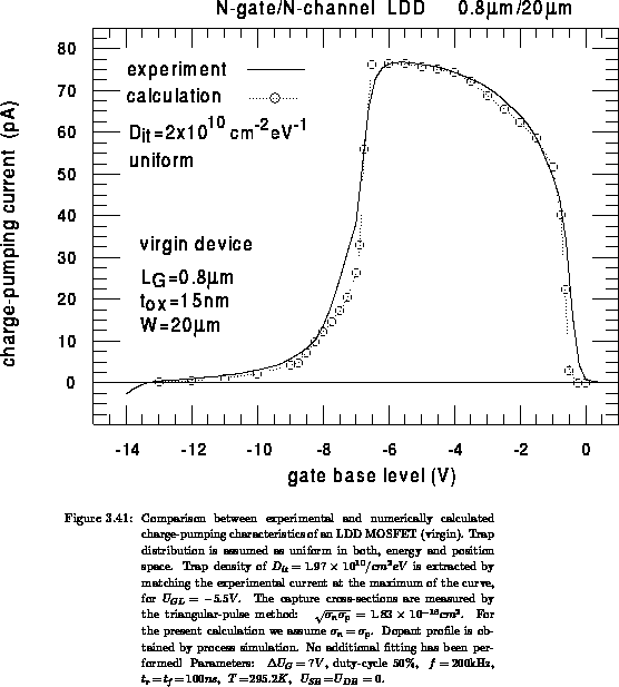
To explain the origin of the first tail in the characteristics of LDD devices, which has no equivalent in the characteristics of conventional MOSFETs, we have compared the numerical calculations with experimental charge-pumping data for an LDD device.
The -channel LDD MOSFET considered in this study:  ,
,
 ,
,  . The drain spacer length is
  .
The two-dimensional doping profile is constructed from three one-dimensional
profiles for the LDD-region, channel and the source/drain junctions, resulting
from SUPREM III simulations [203].
.
The two-dimensional doping profile is constructed from three one-dimensional
profiles for the LDD-region, channel and the source/drain junctions, resulting
from SUPREM III simulations [203].
To convert the one-dimensional profiles of both, LDD and source/drain implants
into the two-dimensional profile a lateral extension factor of  is
assumed. The impurity distribution along
the interface in the gate/LDD overlap region is the most critical part of the
doping profile influencing the accuracy of our analysis. It is most likely,
that this distribution is reproduced only roughly by the rotation of the
one-dimensional profile multiplied by the lateral extension factor.
is
assumed. The impurity distribution along
the interface in the gate/LDD overlap region is the most critical part of the
doping profile influencing the accuracy of our analysis. It is most likely,
that this distribution is reproduced only roughly by the rotation of the
one-dimensional profile multiplied by the lateral extension factor.
To compare the calculation with the experiment, the trap-related parameters are
needed. We assume quite arbitrarily that the traps are acceptor-like and
uniformly distributed in the forbidden gap. We judged that it was reasonable to
assume that the traps are uniformly distributed along the interface.
Nonuniformity has not been observed in carefully applied charge-pumping
measurements on virgin devices [480][398] . It is known from the extensive experimental work that high
dopant concentrations in the bulk can induce traps at the interface of
thermally oxidized doped silicon [441][359]. Since the dopant
concentration in both, the channel and the LDD-region is lower than
. It is known from the extensive experimental work that high
dopant concentrations in the bulk can induce traps at the interface of
thermally oxidized doped silicon [441][359]. Since the dopant
concentration in both, the channel and the LDD-region is lower than
 in our case, we adopt the latter effect as being
small. By matching the maximum of the characteristics, at
in our case, we adopt the latter effect as being
small. By matching the maximum of the characteristics, at
 , a trap density of
  follows.
The capture cross-sections  and
and  are extracted by employing
the triangular-pulse method [154]. This method results in
are extracted by employing
the triangular-pulse method [154]. This method results in
 . Since no experimental data for a separate
determination of and were available, we arbitrarily
assumed
. Since no experimental data for a separate
determination of and were available, we arbitrarily
assumed  and
and  in the
calculation. A ratio
in the
calculation. A ratio  has been estimated by a
spectroscopic charge-pumping technique in [97]. Very large differences
between and , ranging from
has been estimated by a
spectroscopic charge-pumping technique in [97]. Very large differences
between and , ranging from  to
to  times, have
been measured by the three-level technique in [397], but the differences
are reduced to
times, have
been measured by the three-level technique in [397], but the differences
are reduced to  in further work by the same
authors [395][11]. Measurements on -type and
in further work by the same
authors [395][11]. Measurements on -type and  -type MOS
capacitors by the conductance techniques reported in the literature
(see Chapter 7. in [331]) have shown that is larger
than . The ratio ranges from approximately
-type MOS
capacitors by the conductance techniques reported in the literature
(see Chapter 7. in [331]) have shown that is larger
than . The ratio ranges from approximately  to more than
  .
These measurements refer to and in different devices.
Recently developed techniques to measure capture cross-sections associated with
both, electron and hole capture on the same small MOSFET (reviewed in
Section 3.1.1) have shown similar result.
.
These measurements refer to and in different devices.
Recently developed techniques to measure capture cross-sections associated with
both, electron and hole capture on the same small MOSFET (reviewed in
Section 3.1.1) have shown similar result.
 has been found by the conductance technique
in [178]. The measurements employing the split-current method have
given
has been found by the conductance technique
in [178]. The measurements employing the split-current method have
given  in the same MOSFET. As a conclusion, it
seems reasonable to assume that is several times larger than
for a thermally oxidized Si interface, in the same device.
in the same MOSFET. As a conclusion, it
seems reasonable to assume that is several times larger than
for a thermally oxidized Si interface, in the same device.
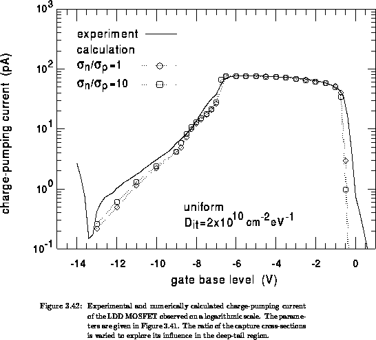
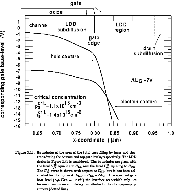
A comparison between the numerical calculation and experiment is given in Figure 3.41. The general agreement is very good. Note that, except for the parameter extraction explained above, no additional fitting has been performed. In particular, two tails at the rising edge of the characteristics has been reproduced by the calculation. However, the agreement between calculation and experiment is not quantitative in these regions, as it is more evident on the logarithmic scale, Figure 3.42.
To gain more insight on the origin of the individual parts of the
characteristics, we analyzed the distribution of the charge-pumping threshold
 and charge-pumping flat-band
  voltages, defined
in Section 3.3. Figure 3.43 shows the
distributions of and along the interface in the
channel, LDD-subdiffusion and the LDD-region. The characteristics
has been shifted downwards on the ordinate by the amount of the pulse amplitude
voltages, defined
in Section 3.3. Figure 3.43 shows the
distributions of and along the interface in the
channel, LDD-subdiffusion and the LDD-region. The characteristics
has been shifted downwards on the ordinate by the amount of the pulse amplitude
 . For a specified base level
  , the area between
both curves determines the region of the total electron and hole capture. This
region completely contributes to
, the area between
both curves determines the region of the total electron and hole capture. This
region completely contributes to  . Without this region the contributions
decay rapidly with the coordinate, to zero.
. Without this region the contributions
decay rapidly with the coordinate, to zero.
From Figure 3.43, it is evident that in the interval


 is influenced mostly by
the intrinsic charge-pumping effect in the channel region
(effect 1. discussed above).
is influenced mostly by
the intrinsic charge-pumping effect in the channel region
(effect 1. discussed above).
 -ray or
  -ray
irradiation [24], in order to mask an eventual nonuniformity in the
virgin device. The method is not capable to provide a full two-dimensional
profile, but is only able to provide the distribution along the interface for
a uniform approximation across the perpendicular coordinate. The potential
applicability, resolution and sensitivity of the measurements may be proven by
means of the numerical simulation of the charge-pumping experiment, before
applying it on real devices. This idea has not been explored in the literature
yet. It is worth to mention that, although important, a reliable and fast
technique to measure the lateral profile in the gate/drain overlap region in
small MOSFETs is still missing. A comprehensive review of the two-dimensional
profile estimation can be found in [448] and references cited there.
-ray
irradiation [24], in order to mask an eventual nonuniformity in the
virgin device. The method is not capable to provide a full two-dimensional
profile, but is only able to provide the distribution along the interface for
a uniform approximation across the perpendicular coordinate. The potential
applicability, resolution and sensitivity of the measurements may be proven by
means of the numerical simulation of the charge-pumping experiment, before
applying it on real devices. This idea has not been explored in the literature
yet. It is worth to mention that, although important, a reliable and fast
technique to measure the lateral profile in the gate/drain overlap region in
small MOSFETs is still missing. A comprehensive review of the two-dimensional
profile estimation can be found in [448] and references cited there.
The numerical calculation is in very good agreement with experimental data in
the second-tail region affected by the fringing effect. The experimental data
shows a change in sign of the current at very low gate base levels, which is
not reproduced by the simulation. An attempt to interpret this effect by
Fowler-Nordheim (F-N) tunneling during the bottom level of the gate pulse
fails, because F-N tunneling will produce a DC component of the same sign
as . A DC component of opposite sign can be attributed to
band-to-band or trap-assisted tunneling in the gate/drain and gate/source
overlap regions, whereas the latter effect probably being dominant in the LDD
device considered here, because the dopant concentration is too low in the
LDD region for the former effect to take place (confirmed by the model described
in Section 4.2).
Tunneling in the bulk, however, does not occur in our experiment, since
the junctions are not biased  . Therefore, the origin
of the change in the current sign in our experimental data still remains
unexplained. Nevertheless, one should always keep in mind that both effects, F-N
tunneling and the tunneling processes in the bulk may modify the result of the
charge-pumping experiments on submicrometer thin-oxide MOSFETs.
. Therefore, the origin
of the change in the current sign in our experimental data still remains
unexplained. Nevertheless, one should always keep in mind that both effects, F-N
tunneling and the tunneling processes in the bulk may modify the result of the
charge-pumping experiments on submicrometer thin-oxide MOSFETs.
Since the region active in the charge pumping becomes very small in the second
tail, we expect that all quantities having an influence on and
may change significantly in this region. The capture
cross-sections and represent such quantities, as
 and
and  depend on them in a direct manner. Numerical
simulation shows, however, that the uncertain ratio
depend on them in a direct manner. Numerical
simulation shows, however, that the uncertain ratio  does
not remarkably affect the ability of our model to match the experimental data
in the deep-tail region, Figure 3.42.
does
not remarkably affect the ability of our model to match the experimental data
in the deep-tail region, Figure 3.42.
In the region  , below the crossover of the and
characteristics shown in Figure 3.43, the
capture of electrons and holes occurs in weak inversion and weak accumulation,
respectively. A two-dimensional transient, consequently a numerical approach
becomes indispensible to model the charge-pumping current in this region. The
spatial coordinate of the crossing point determines the maximal possible depth
to penetrate into the LDD region while scanning the spatial distribution of
interface states (Section 3.5.4). An analytical
model of the gate-corner/LDD-region electrical-field fringing is developed
in Appendix E. It is based on solving the Laplace problem in
the oxide by employing a conformal transformation, assuming equipotential
gate/oxide and semiconductor/oxide surfaces. After obtaining the field
distribution along the oxide/semiconductor interface, we solve the
one-dimensional Poisson equation in the bulk to calculate the charge and surface
potential locally induced. The model may be used for calculation and
qualitative discussion of the fringing effect, but the accurate results can be
obtained by the numerical approach only (cf. Appendix E). From the
analytical model it turns out that rises moderately with decreasing
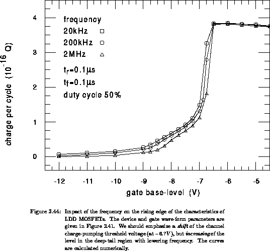
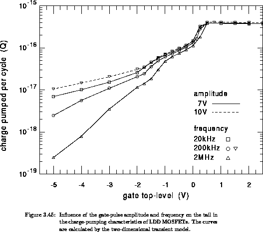
frequency in the deep-tail region. This conclusion is in accord with the
numerical result in Figure 3.44. Increasing the gate-pulse
amplitude is a more efficient way to penetrate into the LDD region than lowering
the frequency, Figure 3.45. These results should be exploited
in charge-pumping measurements.
, below the crossover of the and
characteristics shown in Figure 3.43, the
capture of electrons and holes occurs in weak inversion and weak accumulation,
respectively. A two-dimensional transient, consequently a numerical approach
becomes indispensible to model the charge-pumping current in this region. The
spatial coordinate of the crossing point determines the maximal possible depth
to penetrate into the LDD region while scanning the spatial distribution of
interface states (Section 3.5.4). An analytical
model of the gate-corner/LDD-region electrical-field fringing is developed
in Appendix E. It is based on solving the Laplace problem in
the oxide by employing a conformal transformation, assuming equipotential
gate/oxide and semiconductor/oxide surfaces. After obtaining the field
distribution along the oxide/semiconductor interface, we solve the
one-dimensional Poisson equation in the bulk to calculate the charge and surface
potential locally induced. The model may be used for calculation and
qualitative discussion of the fringing effect, but the accurate results can be
obtained by the numerical approach only (cf. Appendix E). From the
analytical model it turns out that rises moderately with decreasing
frequency in the deep-tail region. This conclusion is in accord with the
numerical result in Figure 3.44. Increasing the gate-pulse
amplitude is a more efficient way to penetrate into the LDD region than lowering
the frequency, Figure 3.45. These results should be exploited
in charge-pumping measurements.