Charge-Pumping Signals in MOSFETs
In this appendix we will present the evolution of the total generation-recombination currents and the terminal currents in a small MOSFET during one period of the gate pulse. We consider large-signal charge pumping with the trapezoidal pulses applied on the gate. All results are obtained by using a selfconsistent numerical model. The signals are qualitatively discussed. Signals in MOS capacitors are modeled in one-dimension by an analytical approach in [435][434][233][232] and numerically in [149][87]. Measured signals can be found in [233][232]. Signals in MOSFETs obtained by an one-dimensional numerical approach are presented in [395][145][144] and by an analytical model in [115]. According to my knowledge, this is the first detailed illustration of the complete processes in the time domain, which occur during the charge pumping in a short-channel MOSFET, obtained by a two-dimensional transient approach.
In this appendix we consider two devices which are also used for the calculations presented in Sections 3.5.1 and 3.5.3:
 -gate/-channel MOSFET, with gate length
 ; effective (metallurgical) channel length
 (junction subdiffusion
  ); junctions
are abrupt (no LDD); oxide thickness
); junctions
are abrupt (no LDD); oxide thickness  ; channel width
 . Acceptor-like traps are assumed uniformly distributed
along the interface and in the energy space (arbitrary); trap density
. Acceptor-like traps are assumed uniformly distributed
along the interface and in the energy space (arbitrary); trap density
 .
.
 and peak location
 . Standard deviation is chosen as
  , giving the
full width at half-maximum of
, giving the
full width at half-maximum of  which is comparable to the oxide
thickness and to the width of the lateral field-peak. To propose the
peak-location
which is comparable to the oxide
thickness and to the width of the lateral field-peak. To propose the
peak-location  , we assumed the stress bias at
  ,
,
 (
( ) and found that the lateral field-peak
is located at
) and found that the lateral field-peak
is located at  . The maximum of the damage is chosen to be located
 away from the field-peak, toward the metallurgical junction,
i.e.
away from the field-peak, toward the metallurgical junction,
i.e.  from the junction. In addition to the field
distribution, the spatial distribution of the electron and hole currents
injected into the oxide are calculated by MINIMOS [172].
At the stress
bias
from the junction. In addition to the field
distribution, the spatial distribution of the electron and hole currents
injected into the oxide are calculated by MINIMOS [172].
At the stress
bias 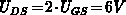 holes are injected in the
interval from
holes are injected in the
interval from  to , whereas the injection current falls
rapidly without this interval. The channel hot-electrons are injected in
a broad interval before the pinch-off point
to , whereas the injection current falls
rapidly without this interval. The channel hot-electrons are injected in
a broad interval before the pinch-off point which is located at
  . After the pinch-off
in the region toward the drain, electrons are injected into the oxide in
a large amount as well, but a significant part of them does not contribute
to the gate current (does not arrive at the gate electrode) due to the
repulsive oxide field and the scattering in the oxide before
approaching the potential maximum. As a conclusion, the position of the
stress-generated traps corresponds approximately to the place
where a significant injection of both, electrons and holes occurs.
and the standard deviation
. After the pinch-off
in the region toward the drain, electrons are injected into the oxide in
a large amount as well, but a significant part of them does not contribute
to the gate current (does not arrive at the gate electrode) due to the
repulsive oxide field and the scattering in the oxide before
approaching the potential maximum. As a conclusion, the position of the
stress-generated traps corresponds approximately to the place
where a significant injection of both, electrons and holes occurs.
and the standard deviation
 , almost all stress-generated traps reside within the drain
junction, but very close to the metallurgical boundary. This fact has
particular consequences on the charge-pumping characteristics.
, almost all stress-generated traps reside within the drain
junction, but very close to the metallurgical boundary. This fact has
particular consequences on the charge-pumping characteristics.
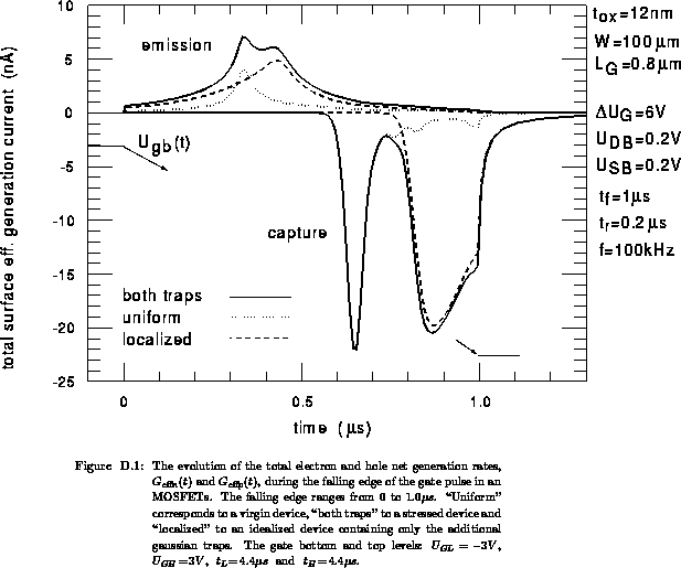
The calculated signals of the total electron and hole net generation rates in
the virgin and the stressed device are presented in
Figure D.1, for the falling edge and in
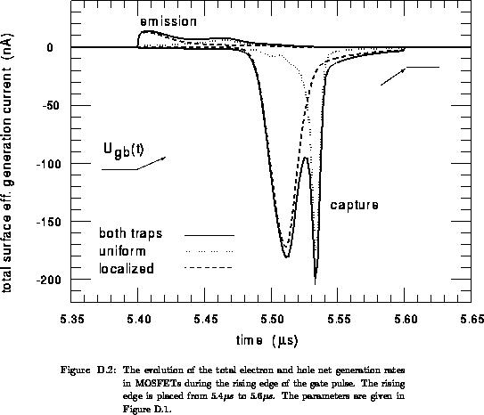
Figure D.2, for the rising edge of the gate pulse. Since the
top level of the trapezoidal pulses is higher than the channel threshold
voltage, the complete interface becomes inverted during the top level. However,
only the interface region from  to approximately is accumulated
during the bottom level, because of a limited penetration into the
junctions (see
Figure 3.22). As a consequence, some of the stress-generated
gaussian distributed traps are not active in charge pumping.
to approximately is accumulated
during the bottom level, because of a limited penetration into the
junctions (see
Figure 3.22). As a consequence, some of the stress-generated
gaussian distributed traps are not active in charge pumping.
The electron emission at the beginning of the falling edge occurs at first in
the steady-state mode, Figure D.1. The emission current is
governed directly by moving the Fermi level of electrons at the interface in
time;  . The traps laying above Fermi level
are emitted. For these traps the emission time constant is shorter than the
capture time constant which depends on the surface concentration
. The traps laying above Fermi level
are emitted. For these traps the emission time constant is shorter than the
capture time constant which depends on the surface concentration
 . depends on the slope
of the gate bias changes. The maximum of the electron emission current
corresponds approximately to the transition from the steady-state to the
non-steady-state emission mode. When the gate bias pass the threshold voltage,
the surface electron concentration and, consequently,
. depends on the slope
of the gate bias changes. The maximum of the electron emission current
corresponds approximately to the transition from the steady-state to the
non-steady-state emission mode. When the gate bias pass the threshold voltage,
the surface electron concentration and, consequently,  fall
rapidly. From this moment the
electron emission current becomes independent of the gate bias changes and
falls to zero obeying a nearly exponential law. The localized gaussian traps
fall
rapidly. From this moment the
electron emission current becomes independent of the gate bias changes and
falls to zero obeying a nearly exponential law. The localized gaussian traps
are assumed to be of acceptor type and in an amount which is sufficient to
increase significantly the local potential (by nearly  ). However,
these traps are emitted after the uniform traps residing mostly in the channel
do, because of a strong fall-off of the local threshold voltage in the junctions
(Figure 3.5.1). Similarly, due to the spatially
variable flat-band potential the capture of holes occurs later for the
traps localized in the junction than for the traps in the channel. The
opposite holds for the electron capture at the rising edge of the gate pulse,
Figure D.2.
). However,
these traps are emitted after the uniform traps residing mostly in the channel
do, because of a strong fall-off of the local threshold voltage in the junctions
(Figure 3.5.1). Similarly, due to the spatially
variable flat-band potential the capture of holes occurs later for the
traps localized in the junction than for the traps in the channel. The
opposite holds for the electron capture at the rising edge of the gate pulse,
Figure D.2.
As evident from the calculation, significant emission and capture take place at the rising and falling edges of the gate pulses, namely when the gate bias varies, while these processes nearly vanish during the bottom and top levels. To explain this fact, let us observe that the total generation-recombination currents in MOSFETs are influenced by two effects while changing the gate bias:
At the beginning of the falling edge, a step in the generation currents occurs.
Note that the complete interface including the junctions is active in the
emission at this moment. Since the emission occurs in the steady-state mode and
 changes suddenly, the emission current exhibits a
step from zero to a finite value. At the end of the falling edge, the amplitude
of the emission current falls rapidly. This decrease is caused by stopping the
broadening of the interface area which becomes active in the emission processes
while decreasing the gate bias, noted as effect 1. above. An additional effect
is that traps in the narrow interface area which has just become active, begin
to emit in the steady-state mode. A sharp change in
at the end of the falling edge causes a step in the
emission current from this area.
changes suddenly, the emission current exhibits a
step from zero to a finite value. At the end of the falling edge, the amplitude
of the emission current falls rapidly. This decrease is caused by stopping the
broadening of the interface area which becomes active in the emission processes
while decreasing the gate bias, noted as effect 1. above. An additional effect
is that traps in the narrow interface area which has just become active, begin
to emit in the steady-state mode. A sharp change in
at the end of the falling edge causes a step in the
emission current from this area.
Both effects noted above modulate the evolution of the total hole and
electron capture currents. While the active localized traps are almost
completely filled by electrons at the rising edge, they are only partially
filled by holes at the falling edge. During the falling edge the penetration of
the accumulation layer into the junction towards the drain causes that more and
more localized traps become captured, thus producing a large hole recombination
current. When the gate bias approaches the bottom level, the penetration
into the junctions stops. Most of the active localized traps have already
been filled by holes, as a consequence of the rapidly increasing hole
concentration. However, traps around the region where the local charge-pumping
flat-band potential equals to the bottom level are not filled. They begin to
capture holes at the beginning of the bottom level ( ). Because the
surface hole concentration is constant, the total recombination current falls
with an exponential law to zero, as is shown in Figure D.1.
). Because the
surface hole concentration is constant, the total recombination current falls
with an exponential law to zero, as is shown in Figure D.1.
The evolution of the total emission and capture currents for electrons and
holes in the stressed device may be nearly represented by a superposition of
the currents for uniform and localized traps. The charge-pumping
current is calculated to be  in the virgin device and
  in an
idealized device which only contains the localized traps. The current in the
stressed device is
in an
idealized device which only contains the localized traps. The current in the
stressed device is  which is very close to the sum of the former two
currents. In this example the DC component of the bulk current differs from the
DC component of the net generation currents of electrons and holes by only about
which is very close to the sum of the former two
currents. In this example the DC component of the bulk current differs from the
DC component of the net generation currents of electrons and holes by only about
 due to the geometric current component and the reverse junction leakage
currents. The fact that the total signal is a superposition of the signals
from the traps residing in the particular interface and volume regions of
the device is a typical peculiarity of the charge-pumping effect.
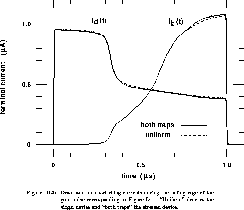
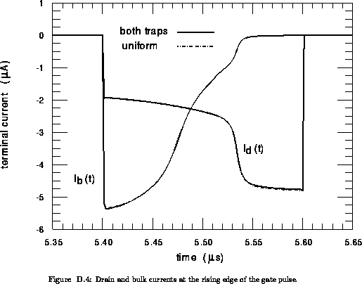
The signals of terminal currents are shown in Figures D.3
and D.4 for the stressed device (both traps) and the virgin
device (uniform). The terminal switching currents are two to three orders of
magnitude larger than the generation-recombination currents. Since we calculate
the charge-pumping current as the DC component of the terminal currents, it is
evident that very accurate calculation of the transient terminal currents is
indispensible for our approach.
due to the geometric current component and the reverse junction leakage
currents. The fact that the total signal is a superposition of the signals
from the traps residing in the particular interface and volume regions of
the device is a typical peculiarity of the charge-pumping effect.
The signals of terminal currents are shown in Figures D.3
and D.4 for the stressed device (both traps) and the virgin
device (uniform). The terminal switching currents are two to three orders of
magnitude larger than the generation-recombination currents. Since we calculate
the charge-pumping current as the DC component of the terminal currents, it is
evident that very accurate calculation of the transient terminal currents is
indispensible for our approach.
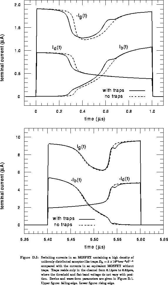
In order to better understand the transient processes in the stressed device against those in the virgin device, we calculate the switching currents for an equivalent device which contains high density uniformly distributed traps in the channel. In this device, the traps are removed away from the junctions; thereby, the signals are not influenced by the geometric effects discussed in 1. In addition, the terminal currents in an equivalent device which does not contain any traps are calculated as well. The results are shown in Figures D.5.
At the falling edge when the localized traps begin to emit (from
 to
to  in Figure D.3) the drain current
 is smaller in the stressed device than in the virgin device. The sum
of the total charge in the inversion layer and the total charge trapped in
interface states is nearly equal in both devices, because it depends primarily
on the effective gate bias. In the virgin device a larger part of the total
charge reside in the channel and a smaller part is trapped in interface states
in comparison with the stressed device. As a consequence, the drain current is
larger in the virgin than in the stressed device while removing the inversion
layer. The effect may be clearly observed in Figure D.5
(upper).
is smaller in the stressed device than in the virgin device. The sum
of the total charge in the inversion layer and the total charge trapped in
interface states is nearly equal in both devices, because it depends primarily
on the effective gate bias. In the virgin device a larger part of the total
charge reside in the channel and a smaller part is trapped in interface states
in comparison with the stressed device. As a consequence, the drain current is
larger in the virgin than in the stressed device while removing the inversion
layer. The effect may be clearly observed in Figure D.5
(upper).
The hole capture on the localized traps increases the bulk current  in
the stressed device with respect to in the virgin device (from
in
the stressed device with respect to in the virgin device (from
 to
to  ). At the beginning of the rising edge, in
the stressed device is slightly larger than the current in the virgin device
due to the hole emission from the localized traps, as is shown in
Figure D.4.
). At the beginning of the rising edge, in
the stressed device is slightly larger than the current in the virgin device
due to the hole emission from the localized traps, as is shown in
Figure D.4.
Electron capture processes at the rising edge can be nicely seen in
Figure D.4. When electrons start to fill the traps which are
not charged by the hole emission, the drain current increases compared with the
device without traps. During the formation of the inversion layer the drain
current in the device with traps is smaller than in the device without traps
because of a smaller inversion-layer charge in the latter device. The net
charge transfer which is represented by the area under the gate-current
signal in one half period, is nearly equal in both devices.