Semiconductor devices have become an ubiquitous commodity and one is used to expect a constant increase of device performance at higher integration densities and falling prices. It is this quest for ever decreasing device dimensions and faster switching speeds that results in ever growing requirements on simulation methodology and thereby on the application design. While computer performance is steadily increasing the additional complexity of these simulation models easily outgrows this gain. This example presents a non-linear problem, discretized by the finite volume method, to show the high expressiveness of the resulting application code.
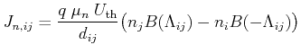
The drift diffusion model which can be derived from Boltzmann's equation by applying the method of moments [132] has been used very successfully in semiconductor device simulations. Equations 8.8 show the resulting current relations. These equations are solved self-consistently by Poisson's equation, given in Equation 8.9.
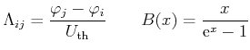
To this end, the equations are discretized using the Scharfetter-Gummel [154] scheme, resulting in a non-linear equation system of the form [132]
 |
(8.10) |
 |
(8.11) |
 |
 |
(8.12) |
The transformation of the presented equations into C++ code is presented in the following source snippet.
![\begin{lstlisting}[frame=lines]{}
// Poisson equation
//
equation_pot =
(
sum<...
...x>()[ pot]/U_th)
) * q * mu_p * U_th * area/dist
]
) (*vit);
\end{lstlisting}](img811.png)
By this transformation a link between the still continuous formulation of the equation and a specific chain complex of the simulation domain is formed. As can be observed, the implementation above makes no assumptions about the dimension of the problem and is therefore suitable for arbitrary dimensions. It should be noted that any scaling in the mathematical sense was not carried out in order to highlight the expressiveness of GSSE in this simple example.
The Bernoulli function, given in Equation 8.11, is mapped to Bern, where the discretized differential operators are easily recognized as the diff and sum constructs. This dimension-independent formulation is made possible only by the combination of the separation of algorithms from data sources by the use of traversal mechanisms (Section 7.1) and by the employment of functional objects (Section 7.2). Here, it is important to highlight that the entire application is available at compile-time and can thereby be highly optimized at once. Calculation results based on the techniques presented are provided in the following section.
To demonstrate that the proposed computational scheme is indeed operational a two-dimensional PN-diode is analyzed. Two neighboring regions of different doping, one doped with acceptors, the other doped with donors, result in the well-known rectifying PN diode. Such a two-dimensional silicon PN-diode is simulated based on the given code section. The complete application uses no more then 200 lines of source code for all different dimensions and topological input structures. Figure 8.14 depicts the input structure for two and three dimensions.
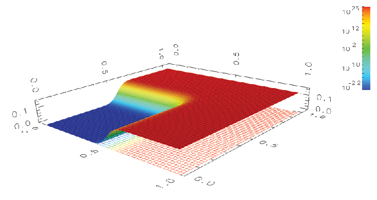
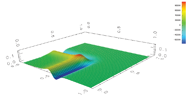
The concentration of acceptors has a maximum of
![]() , the donors concentration has a maximum of
, the donors concentration has a maximum of
![]() . The netto doping profile (
. The netto doping profile (![]() )
of the device presented in
Figure 8.14 is illustrated in
Figure 8.15.
)
of the device presented in
Figure 8.14 is illustrated in
Figure 8.15.
 |
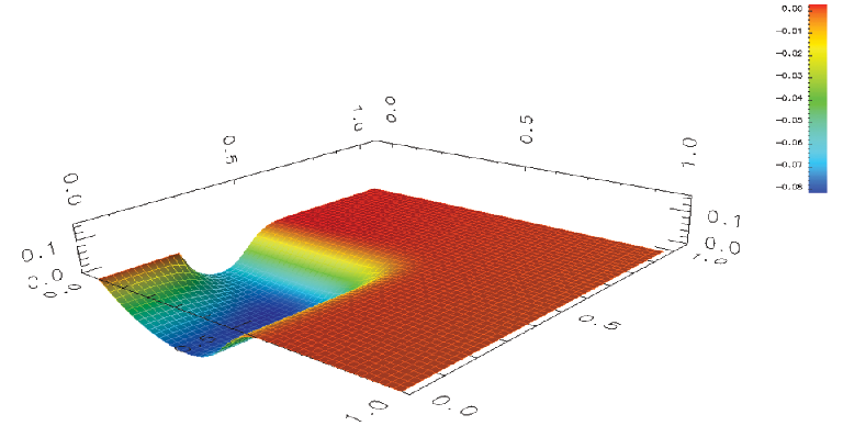
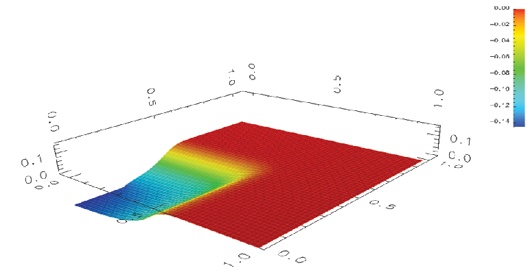
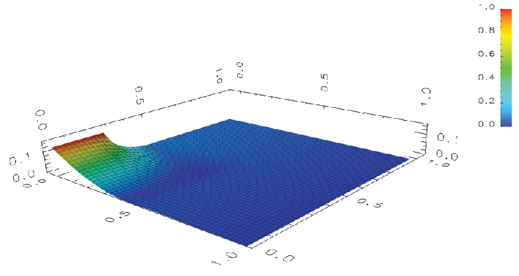
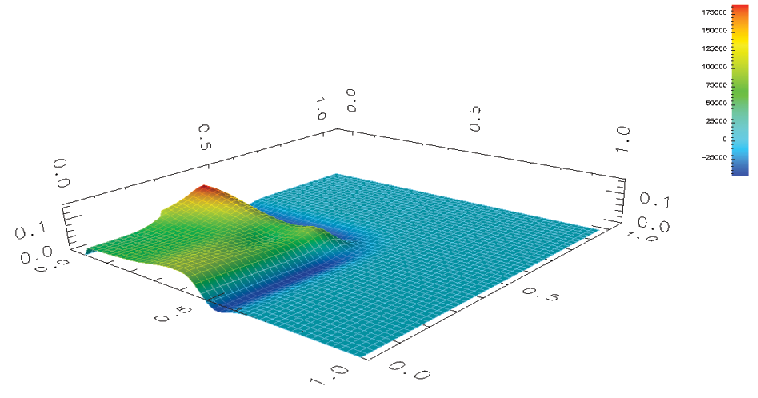
The shape of the initial barrier present without external bias and for reverse mode can be seen in Figure 8.16. When operated in reverse the current is blocked, as is illustrated by the potential when the initial barrier is increased, as shown in Figure 8.17. In forward operation mode, current can run freely, which is reflected by the lowering of the initial potential barrier, as shown in Figure 8.18. The space-charge distribution for reverse mode can be seen in Figure 8.19 and for forward mode in Figure 8.20.
 |
 |
 |
 |
 |
![\begin{figure}\begin{center}
\psfrag{SD} [c]{$\Gamma^D$}
\psfrag{x} [c]{x}
...
...s_device_01_diode.eps, angle=0, width=0.45\textwidth}
\end{center}
\end{figure}](img812.png)