The following examples are a selection of examples with short comments providing a brief description.
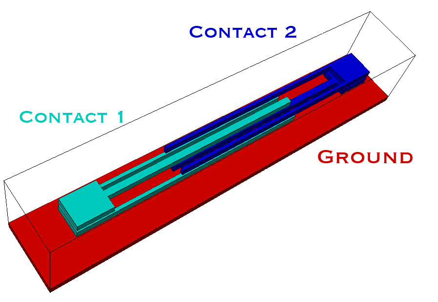
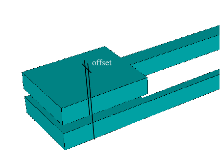
This example not only provides a capacitance extraction for the structure illustrated in Figure 9.2 but also shows how different mesh generation techniques influence the whole simulation process. A LAYGRID mesh and the VGM mesh were used as a calculation base. It is important to highlight that the given structure complicates the original LAYGRID approach, due to the offset of the second layer, depicted in Figure 9.4 on the left side. By a prismatic mesh generation, this issue can result in a mesh with more than two to three orders of magnitude difference in the number of mesh elements. Therefore the example was appropriately adapted to enable the comparison with the LAYGRID mesh approach.
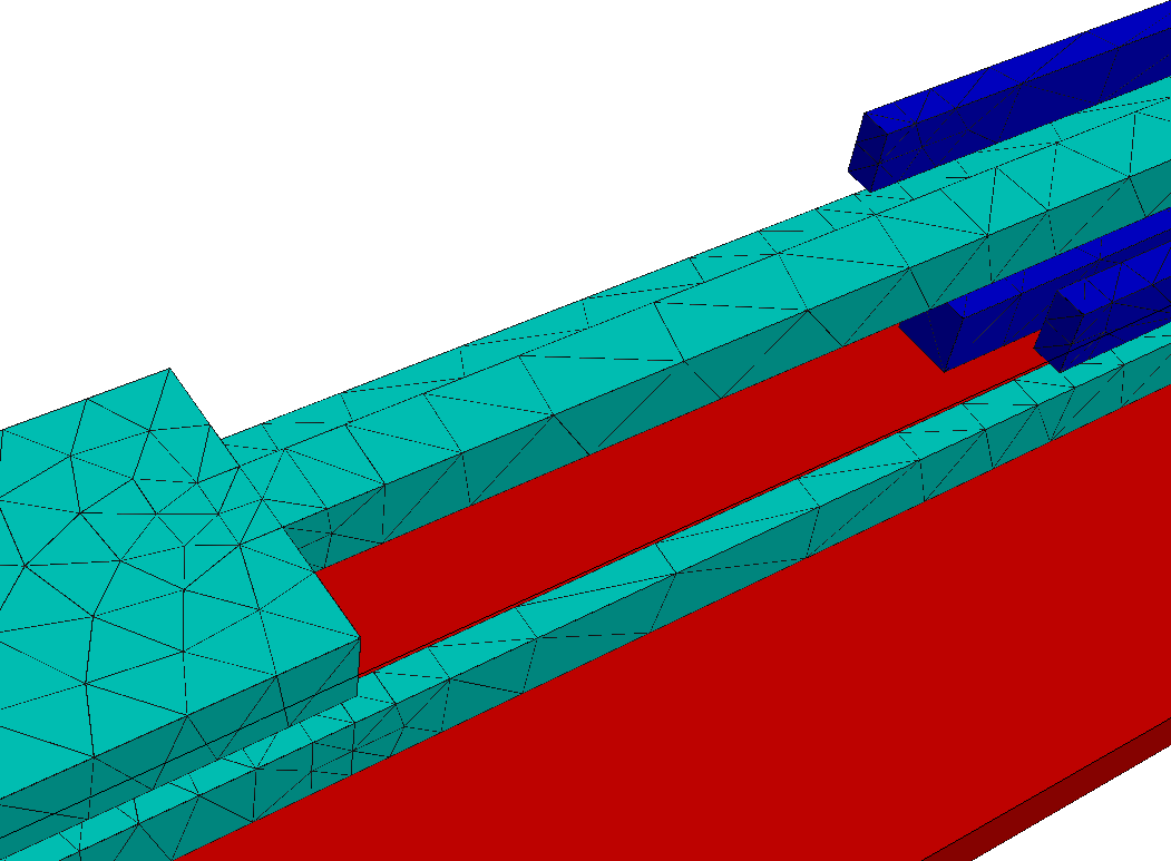
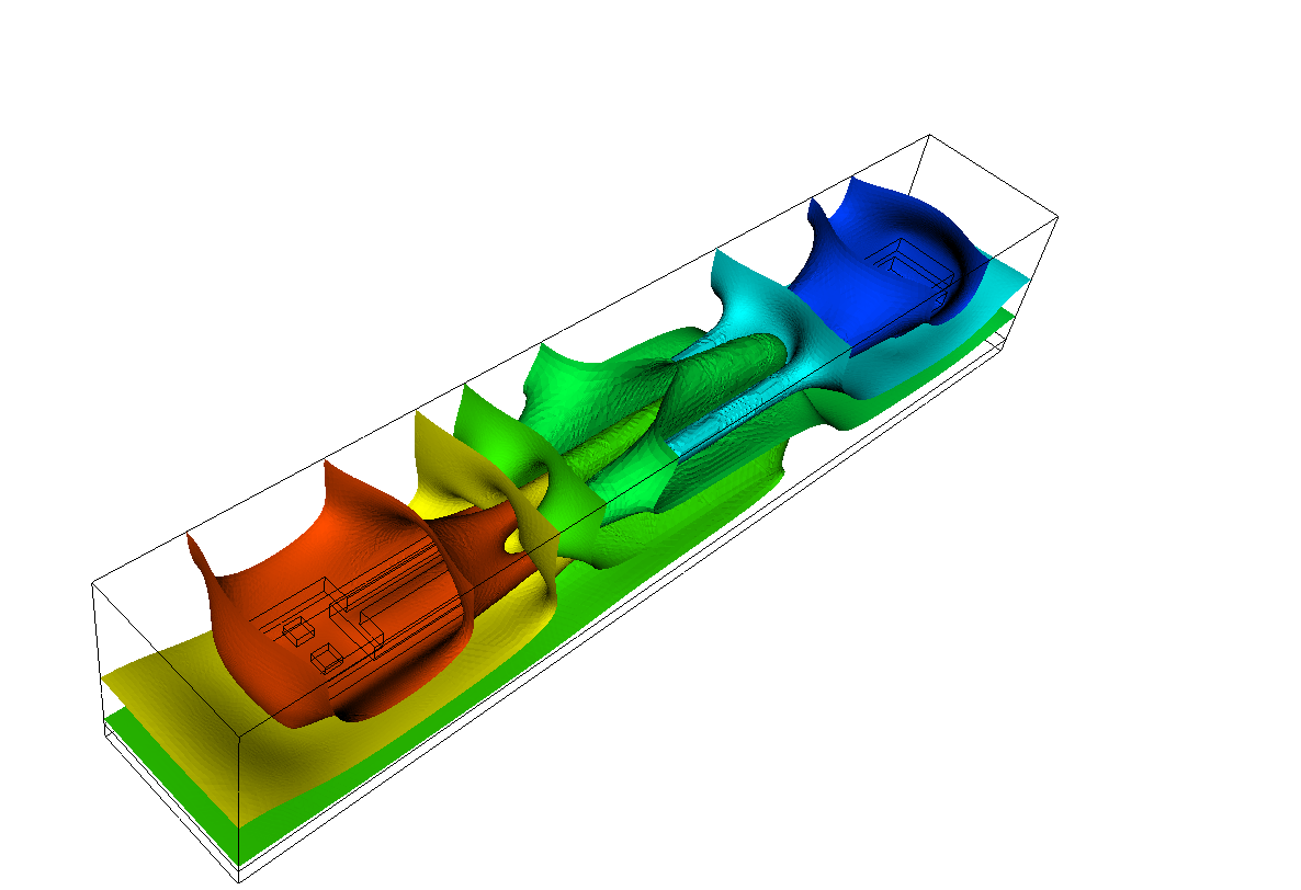
The potential distribution for the two contacts is given in Figure 9.5. A smooth potential is required to extract the capacity correctly. Therefore care has to be taken in regard to spatial discretization of the structure, as shown in Figure 9.4 on the right side.
A capacitance extraction analysis is given in the following table, where the left column always represents the LAYGRID mesh and the right column the VGM mesh. The refinement column states the required overall mesh refinement steps to obtain the targeted accuracy. The x marks examples, where no meshes could be generated.
| Refinement | Capacity [pF] | Number of points | Calculation time [s] | Relative error | ||||
| LAYGRID | VGM | LAYGRID | VGM | LAYGRID | VGM | LAYGRID | VGM | |
| 0 | 5.08 | 22.59 | ||||||
| 2 | 0.07 | 2.44 | ||||||
| 4 | x | x | x | x | 0.0 | |||
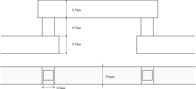
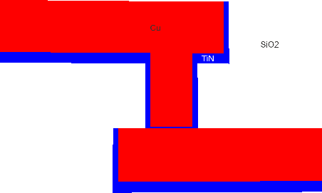
This example deals with the resistance analysis of different types of via structures related to their cross-section in a copper-dual-damascene architecture, illustrated in Figure 9.6. It is shown how the thickness of the barrier layer influences the structure's resistance [114].
Figure 9.7 illustrates the different material types of the structure under investigation as well as the TiN barrier layer.
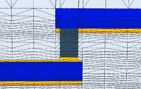
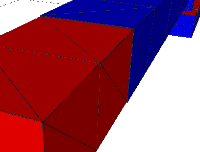
To give a short overview of the new mannerism of VGM a comparison of a LAYGRID structure and a VGM structure is presented next.
|
Figure 9.9:
Left: structure created by LAYGRID . Right: structure created by VGM. With the VGM approach different rations between the interconnect line (red) and the covering layer (blue) can be easily modeled. Here a ratio between the thickness of the interconnect line and the covering layer is given by | |
The influence of the barrier thickness which respect to the overall resistance of the structure can be clearly observed in small cross-sections of the via.
![\begin{figure}\begin{center}
\psfrag{0} [c]{$0$}
\psfrag{1} [c]{$1$}
\psfr...
...ion/interconnect/sap_gsse.ps, angle=-90, width=9.5cm}
\end{center}\end{figure}](img889.png)