Before an implantation the crystalline silicon substrate is often covered by an
amorphous layer, preferably silicon dioxide, to scatter the implanted ions and
to reduce thereby the channeling effect. In the following the scattering
behavior of silicon dioxide (SiO![]() ), silicon nitride (Si
), silicon nitride (Si![]() N
N![]() ) and of
tungsten silicide (WSi
) and of
tungsten silicide (WSi![]() ) is analyzed, by evaluating the influence of the
scattering layers on the motion of boron ions implanted with an energy of 30 keV
and an energy of 90 keV.
) is analyzed, by evaluating the influence of the
scattering layers on the motion of boron ions implanted with an energy of 30 keV
and an energy of 90 keV.
In Fig. 5.1 to Fig. 5.3 the
momentum distribution of the boron atoms leaving the scattering layer is
analyzed. Even if
an ion beam with ions with a single moment is implanted into a scattering layer
the beam of particles leaving the scattering layer becomes divergent. This
means that the distribution of the moments of the particles leaving
the scattering layer is centered around the original ion beam direction, which
is indicated by 0
![]() in the figures Fig. 5.1 to Fig. 5.3.
in the figures Fig. 5.1 to Fig. 5.3.
If the ions were homogeneously distributed the probability ![]() for finding
an ion momentum with an angle
for finding
an ion momentum with an angle ![]() to a reference direction (0
to a reference direction (0
![]() ) is
) is
 |
(5.1) |
In the analysis the thickness of the scattering layer is varied from 0.5 nm to 30 nm to evaluate the scattering efficiency and the influence of the layer thickness on the scattering efficiency. The scattering efficiency of the layer is all the higher the larger the divergence of the ion beam leaving the scattering layer. The scattering efficiency of two materials can be compared by comparing the divergence of the ion beam at a fixed layer thickness.
In Fig. 5.1 the scattering efficiency of SiO![]() is analyzed, while
Fig. 5.2 and Fig. 5.3 demonstrate the scattering
efficiency of Si
is analyzed, while
Fig. 5.2 and Fig. 5.3 demonstrate the scattering
efficiency of Si![]() N
N![]() and WSi
and WSi![]() , respectively. Two ion energies are
analyzed for each material to see if also the ion energy has an influence on the
scattering efficiency.
, respectively. Two ion energies are
analyzed for each material to see if also the ion energy has an influence on the
scattering efficiency.
![\begin{figure}\vspace*{0.5cm}
\begin{center}
\psfrag{Angle \(deg\)}[c][c]{\LARGE...
...hics{fig/appli/SiO2_90/MomentumDist.eps}}}\end{center}\vspace*{-4mm}\end{figure}](img571.gif) |
![\begin{figure}\vspace*{0.5cm}
\begin{center}
\psfrag{Angle \(deg\)}[c][c]{\LARGE...
...ics{fig/appli/Si3N4_90/MomentumDist.eps}}}\end{center}\vspace*{-4mm}\end{figure}](img572.gif) |
|
According to the simulation results the divergence of the scattered ions is all
the higher the thicker the scattering layer is. For instance if Si![]() N
N![]() is
used as a scattering layer and ions with an energy of 90 keV are implanted the
momentum distribution equals the homogeneous momentum distribution at a
scattering angle of 2.2
is
used as a scattering layer and ions with an energy of 90 keV are implanted the
momentum distribution equals the homogeneous momentum distribution at a
scattering angle of 2.2
![]() if the layer thickness is 1 nm, while it equals the
homogeneous momentum distribution at a scattering angle of 6,7
if the layer thickness is 1 nm, while it equals the
homogeneous momentum distribution at a scattering angle of 6,7
![]() if the layer
thickness is 20 nm (Fig. 5.2 (bottom)).
if the layer
thickness is 20 nm (Fig. 5.2 (bottom)).
Additionally it can be said that besides the layer thickness also the ion energy
has an influence on the scattering efficiency. By decreasing the energy of the
ions the scattering efficiency increases. For instance, the probability for
finding an ion scattered by an angle of 2,5
![]() is 1.4 times higher for an
implantation energy of 30 keV than for an implantation energy of 90 keV, if a
3 nm thick WSi
is 1.4 times higher for an
implantation energy of 30 keV than for an implantation energy of 90 keV, if a
3 nm thick WSi![]() scattering layer is used (Fig. 5.3).
scattering layer is used (Fig. 5.3).
Comparing the materials SiO![]() , Si
, Si![]() N
N![]() and WSi
and WSi![]() it can be said
that WSi
it can be said
that WSi![]() has the highest scattering capability while SiO
has the highest scattering capability while SiO![]() has the lowest
scattering capability. While a WSi
has the lowest
scattering capability. While a WSi![]() layer with a thickness of more than 10 nm
is sufficient to achieve an almost homogeneous momentum distribution if the
implantation energy is 30 keV, a SiO
layer with a thickness of more than 10 nm
is sufficient to achieve an almost homogeneous momentum distribution if the
implantation energy is 30 keV, a SiO![]() layer of even 30 nm is not
sufficient. Layer thicknesses of approximately 20 nm SiO
layer of even 30 nm is not
sufficient. Layer thicknesses of approximately 20 nm SiO![]() , 4 nm Si
, 4 nm Si![]() N
N![]() and 3 nm WSi
and 3 nm WSi![]() are comparable in their angular scattering capabilities.
are comparable in their angular scattering capabilities.
As indicated by Fig. 5.4 the stopping behavior of all scattering layers
is similar to the angular scattering capability. Fig. 5.4 shows the
maximum energy ![]() of the ions leaving the scattering layer related to the
implantation energy
of the ions leaving the scattering layer related to the
implantation energy ![]() . WSi
. WSi![]() has the highest stopping capability while
SiO
has the highest stopping capability while
SiO![]() has the lowest stopping capability of the considered materials. The
stopping capability of Si
has the lowest stopping capability of the considered materials. The
stopping capability of Si![]() N
N![]() lies in between. Since the stopping power in
the scattering layer is dominated by the electronic stopping (Sec. 3.3.1)
as well for boron ions with an energy of 30 keV and of 90 keV, the relative
energy of the scattered ions is higher for ions implanted with an energy of
90 keV (Fig. 5.4).
lies in between. Since the stopping power in
the scattering layer is dominated by the electronic stopping (Sec. 3.3.1)
as well for boron ions with an energy of 30 keV and of 90 keV, the relative
energy of the scattered ions is higher for ions implanted with an energy of
90 keV (Fig. 5.4).
The reason is that the relative energy of an ion after scattering is
 |
(5.2) |
| (5.3) |
 |
(5.4) |
![\begin{figure}\begin{center}
\psfrag{Relative Maximal Energy}[c][c]{\LARGE\sf Re...
...{0}{\includegraphics{fig/appli/Emax.eps}}}\end{center}\vspace*{-4mm}\end{figure}](img577.gif) |
![\begin{figure}\begin{center}
\psfrag{Relative Average Energy}[c][c]{\LARGE\sf Re...
...x{0}{\includegraphics{fig/appli/Eav.eps}}}\end{center}\vspace*{-4mm}\end{figure}](img578.gif) |
According to Fig. 5.5 to Fig. 5.8 as well as the momentum distribution, the energy distribution is broadened by increasing the layer thickness or by using a material with a higher scattering capability. Fig. 5.5 shows the difference of the average energy and the maximum energy related to the maximum energy according to (5.5).
![\begin{figure}\vspace*{0.5cm}
\begin{center}
\psfrag{Relative Energy}[c][c]{\LAR...
...aphics{fig/appli/SiO2_90/EnergyDist.eps}}}\end{center}\vspace*{-4mm}\end{figure}](img580.gif) |
|
|
In Fig. 5.6 to Fig. 5.8 the energy distributions of the
boron ions leaving the scattering layer are shown. The energy
distribution is presented by a cumulative sum as a function of the relative
energy
![]() compared to the maximal energy
compared to the maximal energy ![]() of an ion
leaving the scattering layer. Using Fig. 5.6 to Fig. 5.8
the scattering capabilities of the various materials (SiO
of an ion
leaving the scattering layer. Using Fig. 5.6 to Fig. 5.8
the scattering capabilities of the various materials (SiO![]() , Si
, Si![]() N
N![]() and
WSi
and
WSi![]() ) can be analyzed in detail. As for the evaluation of the momentum
distribution two implantation energies are considered for analyzing the energy
distributions for each scattering material type.
) can be analyzed in detail. As for the evaluation of the momentum
distribution two implantation energies are considered for analyzing the energy
distributions for each scattering material type.
The influence of the layer thickness and of the implantation energy on the
energy distributions of the boron ions leaving the scattering layer is
equivalent to the influence on the momentum distribution. As well by increasing the
thickness of the scattering layer as by reducing the implantation energy, the
energy distribution is broadened. Additionally the energy distribution is
broadened by using a material with a higher scattering capability. For instance
if the boron ions are implanted with an energy of 90 keV through a scattering
layer with a thickness of 30 nm approximately 77% of all ions are within an
energy interval of 1% around the maximal energy if the scattering layer
material is SiO![]() , while just 62% and 41% of the ions are within this
interval if the scattering layer material is Si
, while just 62% and 41% of the ions are within this
interval if the scattering layer material is Si![]() N
N![]() or WSi
or WSi![]() respectively.
respectively.
The influence of the scattering layers on the channeling behavior of the ions in
the crystalline silicon substrate and thereby on the distribution of the
implanted atoms is shown in Fig. 5.9 to
Fig. 5.14 for implantations with energies of 30 keV and
90 keV and a dose of
![]() cm
cm![]() . The implantations are performed on the one
hand side with an ion beam tilted by 7
. The implantations are performed on the one
hand side with an ion beam tilted by 7![]() and on the other hand side with
an ion beam aligned with the
and on the other hand side with
an ion beam aligned with the ![]() 100
100![]() crystal direction.
crystal direction.
In case of an implantation along the ![]() 100
100![]() channeling direction as shown for
instance in the bottom figure of Fig. 5.9 the depth of the implanted
profile is successively reduced by increasing the thickness of the scattering
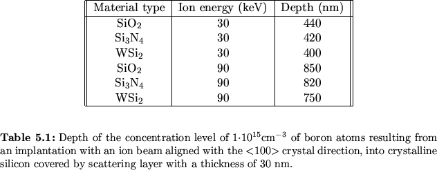
layer. Tab. 5.1 summarizes the depth of the concentration level
of
channeling direction as shown for
instance in the bottom figure of Fig. 5.9 the depth of the implanted
profile is successively reduced by increasing the thickness of the scattering
layer. Tab. 5.1 summarizes the depth of the concentration level
of
![]() cm
cm![]() after an implantation through a scattering layer with a
thickness of 30 nm. Various scattering materials and two implantation energies are
used. A depth of 0 nm in Fig. 5.9 to
Fig. 5.14 and in Tab. 5.1 corresponds to the surface
of the silicon substrate. The values of the depth in Tab. 5.1 are extracted
from the top figures in Fig. 5.9 to
Fig. 5.14.
after an implantation through a scattering layer with a
thickness of 30 nm. Various scattering materials and two implantation energies are
used. A depth of 0 nm in Fig. 5.9 to
Fig. 5.14 and in Tab. 5.1 corresponds to the surface
of the silicon substrate. The values of the depth in Tab. 5.1 are extracted
from the top figures in Fig. 5.9 to
Fig. 5.14.
![\begin{figure}\begin{center}
\psfrag{Depth \(um\)}[c][c]{\LARGE\sf Depth ($\math...
...s{fig/appli/SiO2_30/B_Profile_ch100.eps}}}\end{center}\vspace*{-4mm}\end{figure}](img583.gif) |
|
|
|
|
|
 |
 |
If the ion beam is tilted by 7
![]() the ions first penetrate deeper into the
target if the thickness of the scattering layer is increased, because the
probability that an ion is scattered into a channel increases as shown in
Fig. 5.1 to Fig. 5.3. At a certain scattering layer
thickness the penetration depth reaches a maximum until it decreases
again. If thick scattering layers are used the impurity distributions become
independent on the tilt of the ion beam. To achieve that a thickness of 30 nm,
which is the largest layer thickness in the analysis presented here is
sufficient as well for an implantation with an energy of 30 keV and of 90 keV
and for all scattering layer materials analyzed. Since the effects observed do not
depend on the material type of the scattering layer a
presentation just of Fig. 5.9 would be sufficient, but
Fig. 5.10, Fig. 5.11,
Fig. 5.12, Fig. 5.13 and
Fig. 5.14 are added for the sake of completeness. In this
series of figures first the tilt angle then the material type and finally the
implantation energy is varied.
the ions first penetrate deeper into the
target if the thickness of the scattering layer is increased, because the
probability that an ion is scattered into a channel increases as shown in
Fig. 5.1 to Fig. 5.3. At a certain scattering layer
thickness the penetration depth reaches a maximum until it decreases
again. If thick scattering layers are used the impurity distributions become
independent on the tilt of the ion beam. To achieve that a thickness of 30 nm,
which is the largest layer thickness in the analysis presented here is
sufficient as well for an implantation with an energy of 30 keV and of 90 keV
and for all scattering layer materials analyzed. Since the effects observed do not
depend on the material type of the scattering layer a
presentation just of Fig. 5.9 would be sufficient, but
Fig. 5.10, Fig. 5.11,
Fig. 5.12, Fig. 5.13 and
Fig. 5.14 are added for the sake of completeness. In this
series of figures first the tilt angle then the material type and finally the
implantation energy is varied.
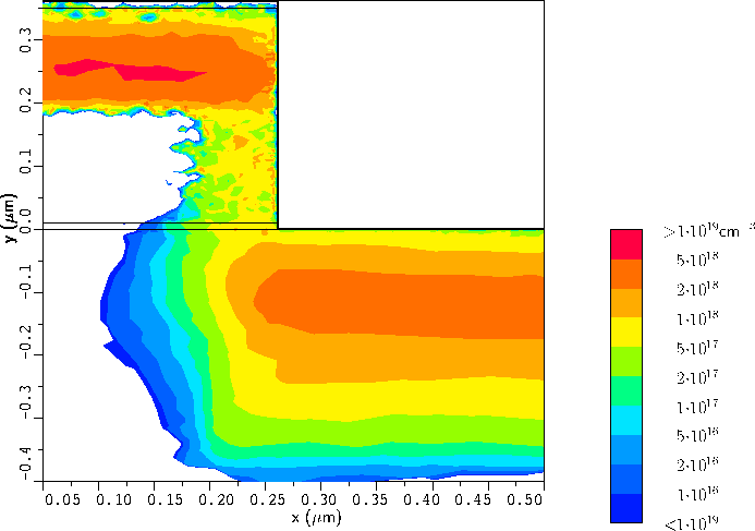
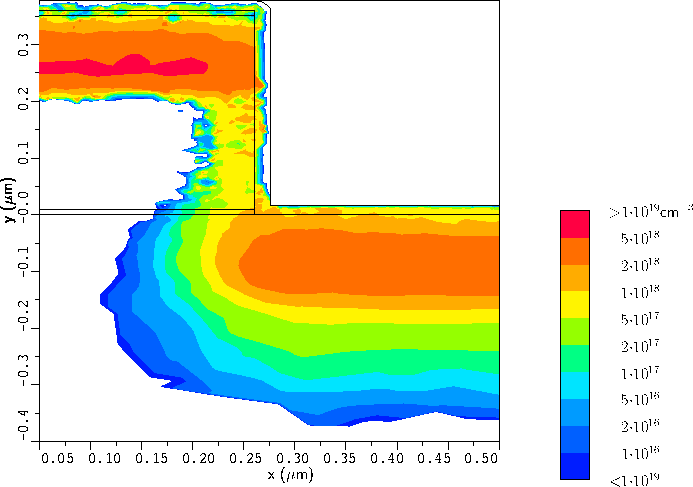
In order to demonstrate that such an analysis is not restricted to one-dimensional problems, the effect of a silicon dioxide scattering layer on the doping profile in the vicinity of a gate corner of a MOS transistor is shown in Fig. 5.15. The scattering layer covers the whole surface and has a thickness of 1 nm in the top figure and of 16 nm in the bottom figure.
Boron ions with an energy of 30 keV and a dose of
![]() cm
cm![]() were implanted into
this structure. The ion beam was tilted by 10
were implanted into
this structure. The ion beam was tilted by 10
![]() to move the boron
atoms slightly under the gate.
to move the boron
atoms slightly under the gate.
By using a thicker scattering oxide the shape of
the doping profile below the gate corner changes from a rectangular shaped
structure to a circular shaped structure. Additionally a shallower doping profile
is generated by implanting through a scattering oxide with a thickness of
16 nm. The iso-concentration line of
![]() cm
cm![]() has a depth of approximately
280 nm and its maximal distance from the gate corner is 90 nm. In case of an
implantation through a scattering layer with a thickness of just 1 nm the depth
of the iso-concentration line of
has a depth of approximately
280 nm and its maximal distance from the gate corner is 90 nm. In case of an
implantation through a scattering layer with a thickness of just 1 nm the depth
of the iso-concentration line of
![]() cm
cm![]() is 355 nm and the distance from
the corner is 100 nm. Therefore the aspect ratios of the doping profiles are 3.1
and 3.55 respectively.
is 355 nm and the distance from
the corner is 100 nm. Therefore the aspect ratios of the doping profiles are 3.1
and 3.55 respectively.
![]()
![]()
![]()
![]() Previous: 5. Applications
Up: 5. Applications
Next: 5.2 Effect of Pre-amorphization
Previous: 5. Applications
Up: 5. Applications
Next: 5.2 Effect of Pre-amorphization