Another method to reduce the channelling effect is to perform two ion implantations immediately one after the other without an annealing step in between. The first implantation is used to destroy the crystalline structure of the substrate. For the implantation ion species are used which are not electrically active. Otherwise a very high doping concentration would be generated due to the high implantation dose which is necessary to achieve an amorphization. Silicon and germanium are the preferred ion species. The second implantation introduces the required dopant atoms.
Fig. 5.16 and Fig. 5.17 demonstrate the
influence of the amorphization by the first implantation on the doping profile
generated by the second implantation. For this analysis the pre-amorphization
was performed by silicon ions with energies ranging from 50 keV to 400 keV.
Additionally the dose is varied in Fig. 5.16 and
Fig. 5.17, from
![]() cm
cm![]() to
to
![]() cm
cm![]() . Finally the dopant
atoms are introduced by a boron ion implantation with an energy of 90 keV.
. Finally the dopant
atoms are introduced by a boron ion implantation with an energy of 90 keV.
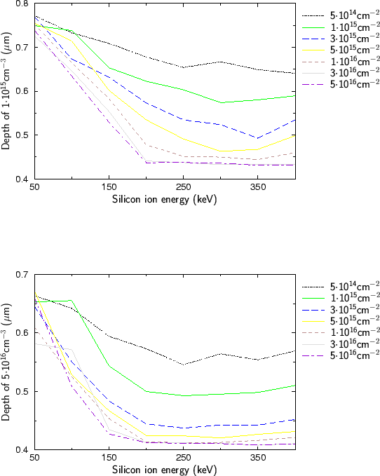
According to the simulation results the penetration depth of the boron
ions is reduced by increasing the energy and the dose of the first
implantation. The change in the penetration depth saturates as well by
increasing the dose as the energy above a certain threshold level as shown in
Fig. 5.18. The top figure of Fig. 5.18 shows
the depth of a concentration level of
![]() cm
cm![]() , while the bottom figure
shows the depth of a concentration level of
, while the bottom figure
shows the depth of a concentration level of
![]() cm
cm![]() as a function of the
ion energy for various doses of the silicon implantation. This saturation effect
can be explained by a useful limit in the size of the amorphous area. The
maximal useful size of the amorphous area is of the order of the penetration
depth of the ions of the second implantation.
as a function of the
ion energy for various doses of the silicon implantation. This saturation effect
can be explained by a useful limit in the size of the amorphous area. The
maximal useful size of the amorphous area is of the order of the penetration
depth of the ions of the second implantation.
![\begin{figure}\begin{center}
\psfrag{Depth \(um\)}[c][c]{\LARGE\sf Depth ($\math...
...\includegraphics{fig/appli/Pre_1e15.eps}}}\end{center}\vspace*{-4mm}\end{figure}](img585.gif) |
![\begin{figure}\begin{center}
\psfrag{Depth \(um\)}[c][c]{\LARGE\sf Depth ($\math...
...\includegraphics{fig/appli/Pre_1e16.eps}}}\end{center}\vspace*{-4mm}\end{figure}](img586.gif) |
 |
 |
 |
By increasing the dose, first the size of the amorphous area increases, staring from a small area around the peak of the point defect distribution, which is close to the peak of the distribution of the implanted silicon ions. Until the amorphous area reaches the surface of the substrate the size of the amorphous area changes quite rapidly by increasing the dose. At higher doses the amorphous area still slightly extends to the maximal penetration depth of the silicon ions.
By increasing the energy mainly the depth of the center of the amorphous area is moved deeper into the target. As long as the amorphous area is smaller than and lies within the range of the atoms of the second implantation, a dependence of the distribution of the atoms of the second implantation on the energy and the dose of the first implantation can be observed.
This explains why the influence of the dose of the first implantation increases
until an implantation energy of 200 keV as show in Fig. 5.18. At
this energy the center of the amorphous area lies
approximately at the same depth as the peak of the boron distribution. The
maximal useful dose of the silicon implantation is about
![]() cm
cm![]() . At this
dose the amorphous area has filled the whole useful area. A further increase of
the dose just extends the amorphous area outside of the useful area and has
therefore no influence on the distribution of the boron ions.
. At this
dose the amorphous area has filled the whole useful area. A further increase of
the dose just extends the amorphous area outside of the useful area and has
therefore no influence on the distribution of the boron ions.
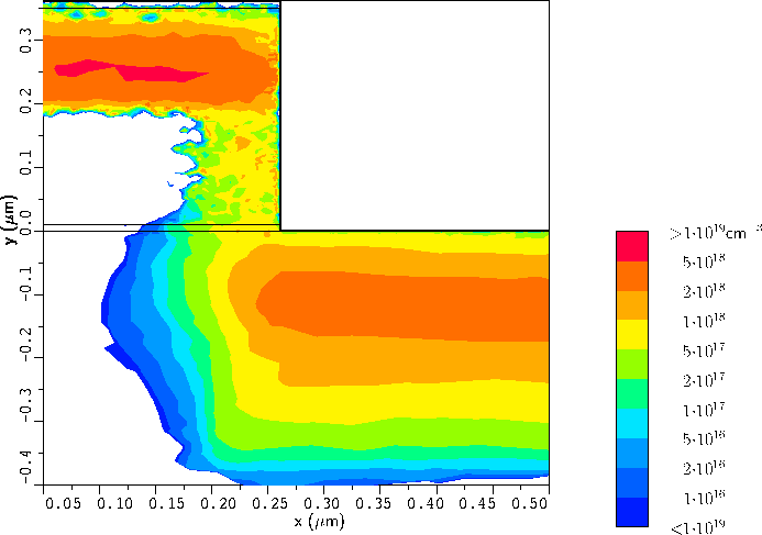
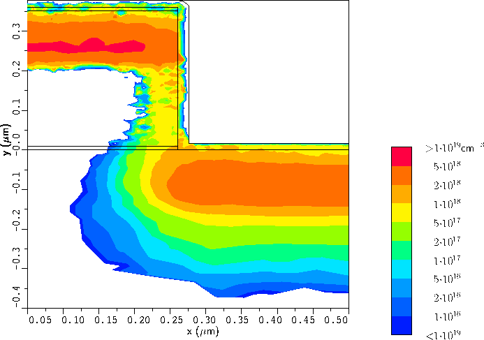
The influence of pre-amorphization on the shape of the doping profile in the
vicinity of a gate corner is studied in Fig. 5.19. An
implantation with boron ions into a MOS transistor structure after the formation
of the spacer is performed with (bottom) and without (top) pre-amorphization by an
implantation with silicon ions. The boron ions are implanted with an energy of
80 keV and a dose of
![]() cm
cm![]() , and the silicon ions are implanted with an
energy of 200 keV and a dose of
, and the silicon ions are implanted with an
energy of 200 keV and a dose of
![]() cm
cm![]() . While the vertical shape and the
depth of the peak of the doping profile remains almost unchanged, the gradient
in the tail region is significantly increased as expected already from the
one-dimensional simulations. The distance of the iso-concentration line of
. While the vertical shape and the
depth of the peak of the doping profile remains almost unchanged, the gradient
in the tail region is significantly increased as expected already from the
one-dimensional simulations. The distance of the iso-concentration line of
![]() cm
cm![]() from the gate corner is 125 nm for the boron implantation without
pre-amorphization while it is 140 nm for the implantation after
pre-amorphization, if the lateral size of the spacer is 72 nm. Without
pre-amorphization the depth of this iso-concentration line is 545 nm and with
pre-amorphization the depth is 365 nm. This results in an aspect ratio of 4.36
and 2.6 respectively. The peak of the boron concentration is approximately at a
depth of 240 nm in both cases.
from the gate corner is 125 nm for the boron implantation without
pre-amorphization while it is 140 nm for the implantation after
pre-amorphization, if the lateral size of the spacer is 72 nm. Without
pre-amorphization the depth of this iso-concentration line is 545 nm and with
pre-amorphization the depth is 365 nm. This results in an aspect ratio of 4.36
and 2.6 respectively. The peak of the boron concentration is approximately at a
depth of 240 nm in both cases.
![]()
![]()
![]()
![]() Previous: 5.1 Effect of Scattering
Up: 5. Applications
Next: 5.3 Pollution of Silicon
Previous: 5.1 Effect of Scattering
Up: 5. Applications
Next: 5.3 Pollution of Silicon