


Next: 3.3 Modeling of Technology
Up: 3.2 Practical Characterization
Previous: 3.2.2 Point Optimization of
The lumped parameter model uses a simple but very fast photographic model
to relate the development time to exposure [53,54]. Based
on the assumption of a constant contrast (3.1) can be integrated
to give a simple expression for the development rate,
 |
(3.4) |
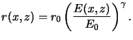
Here, E(x, z) refers to the exposure energy inside the resist and is
related to the normalized aerial image Ii(x) by
E(x, z) = Ew Ii(x) Ir(z).
Ew denotes the exposure energy needed to generate a feature of width w
and Ir(z) is the relative, vertically
z-dependent intensity variation inside the resist.a
The integration constants E0 and r0 are, respectively, the energy
required to exactly clear (w = 0) the photoresist in the allotted development
time and the development rate resulting from an exposure of this amount.
Another parameter of the lumped parameter model is the effective
resist thicknessb
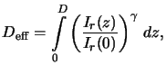 |
(3.5) |
with D as actual resist thickness. The ``effective'' resist
thickness weights the actual height by a term related to
the change in the development rate varying from the top to the bottom
of the film. In case of absorption the development rate is smaller at the
bottom so that the resist film seems to be thicker as it is in reality, i.e.,
a thinner effective resist is required to be cleared in the same time.
Using a phenomenological two-step development model which is
based on the assumption that development occurs first vertically and then
horizontally [55], the two segment times
can be calculated from (3.4). The sum of these two
times equals the total development time and the following expression
is derived:c
![$\displaystyle \frac{E_w}{E_0} = \left[ 1+ \frac{1}{D_\mathrm{eff}} \int\limits_...
...)^{-\gamma}\, dx\right]^{\scriptstyle\frac{\scriptstyle1}{\scriptstyle\gamma}}.$](img269.gif) |
(3.6) |
Note that Ew stands for the required exposure dose to generate a line of
width w, and E0 refers to full resist removal.
(3.6) determines the
required exposure dose Ew to produce a feature of width w for
a given aerial image intensity Ii(x). The two parameters of the model,
the effective resist thickness
Deff and the contrast  ,
are routinely available in most production and
development lithography processes. Hence, linewidth versus exposure
curves can be generated extremely fast by means of simulation.
This simple model can be used as an initial predictor of results or
as the engine of a lithography control scheme.
,
are routinely available in most production and
development lithography processes. Hence, linewidth versus exposure
curves can be generated extremely fast by means of simulation.
This simple model can be used as an initial predictor of results or
as the engine of a lithography control scheme.
Footnotes
- ... thickness,0
-
- ... resist.a
- Originally,
in (3.1) the z-dependence of the development rate was
suppressed. However, for the following considerations it is important. Various
simple methods to compute Ir(z) are described in
Section 5.2.
- ... thicknessb
- The effective resist thickness is defined
as
Deff = r(x, D) tdev, where D is the resist height,
r(x, D) the development rate at the resist bottom, and
tdev the
development time. Integration of the rate equation
dt = r-1(x, z) dz
yields
tdev = r0-1
 (E(x, z)/E0)-
  dz,
whereby (3.4) was inserted. The expression for the
effective resist thickness
Deff is now found by a combination of its
definition with (3.4).
dz,
whereby (3.4) was inserted. The expression for the
effective resist thickness
Deff is now found by a combination of its
definition with (3.4).
- ... derived:c
- The vertical development time follows from
the definition of the effective resist
thickness,0
tz = Deff/r(0, D).
The horizontal development time is obtained from integration of the rate
equation
dt = r-1(x, z) dx and writes to
tx = r0-1
 (E(x, z)/E0)-
  dx.
Summing up the two times yields
tdev = Deff/r(0, D)
dx.
Summing up the two times yields
tdev = Deff/r(0, D) 1 + D-1eff
 (Ii(x)/Ii(0))-
  dx
dx![$ \Big]$](img267.gif) and combines with
(Ew/E0)
and combines with
(Ew/E0) = tdevr(0, D)/Deff
to the provided formula.
= tdevr(0, D)/Deff
to the provided formula.
Next: 3.3 Modeling of Technology
Up: 3.2 Practical Characterization
Previous: 3.2.2 Point Optimization of
Heinrich Kirchauer, Institute for Microelectronics, TU Vienna
1998-04-17