Previous: 4.4.3 Triple-Gate FinFET Up: 4.4 FinFET Next: 5. Summary and Outlook
If a very thin fin is used hard limits of gate length scaling are reached. The off-state current will be comprised by terms such as quantum mechanical tunneling or band-to-band tunneling [180].
Short channel effects can be controlled if
![]() [168,180,181]. When the fin width
[168,180,181]. When the fin width
![]() is reduced, leakage currents in the middle of the fin are
reduced. Thus, the off-state current is reduced and short channel effects
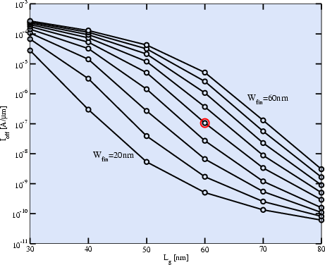
are minimized as shown in Fig. 4.31. The fat point
denotes the device analyzed in Section 4.4.2. To
obtain a lower off-state current, the device width must be reduced. E.g., a
smaller device with a comparable off-state current must have a fin width of
is reduced, leakage currents in the middle of the fin are
reduced. Thus, the off-state current is reduced and short channel effects
are minimized as shown in Fig. 4.31. The fat point
denotes the device analyzed in Section 4.4.2. To
obtain a lower off-state current, the device width must be reduced. E.g., a
smaller device with a comparable off-state current must have a fin width of
![]() and a printed gate length of
approximately
and a printed gate length of
approximately
![]() .
.
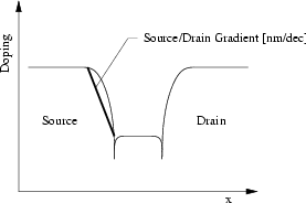
The device is very sensitive to the gate underlap ![]() and the lateral
source/drain doping gradient [180] of the doping profile at the
junctions. For the FinFET simulations a source/drain doping concentration of
and the lateral
source/drain doping gradient [180] of the doping profile at the
junctions. For the FinFET simulations a source/drain doping concentration of
![]() has been assumed. The doping
profile at the junctions have a Gaussian shape. The source/drain gradient
defined in Fig. 4.32 according to [180] was set
to
has been assumed. The doping
profile at the junctions have a Gaussian shape. The source/drain gradient
defined in Fig. 4.32 according to [180] was set
to
![]() . For all simulations a gate underlap of
. For all simulations a gate underlap of
![]() was used. Therefore the effective gate
length is assumed to be fixed at
was used. Therefore the effective gate
length is assumed to be fixed at
![]() .
.
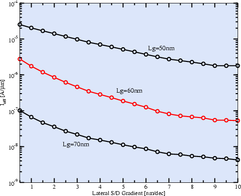
Fig. 4.33 shows the dependency of the off-state current on the lateral source/drain gradient. A higher source/drain gradient reduces the drain induced barrier lowering effect [182,183] and therefore the off-state current. For a fixed off-state current smaller gate lengths are possible in combination with a higher source/drain gradient. Nevertheless, a higher source/drain gradient introduces a series resistance which may severely degrade the on-state current [180].
Robert Klima 2003-02-06