Previous: 4.4.2 Simulation Results Up: 4.4 FinFET Next: 4.4.4 Gate Length Scaling
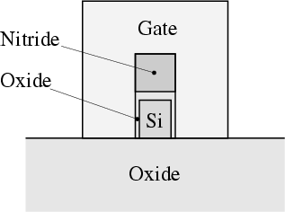
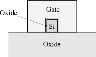
Due to the thick silicon nitride cap on the top of the fin the influence of the top gate can be neglected and the FinFET can be termed a double-gate device (see Fig. 4.21). If the silicon nitride cap is removed a third gate is formed at the top of the fin. This situation is shown in a vertical cut through the fin in Fig. 4.27(b) where Fig. 4.27(a) shows the conventional double-gate structure simulated before.
When the fin width
![]() is much larger than its height
is much larger than its height
![]() or the gate oxide at the top is much thinner than the gate
oxides at the sidewalls the device can be treated as a single gate structure.
Contrary, if
or the gate oxide at the top is much thinner than the gate
oxides at the sidewalls the device can be treated as a single gate structure.
Contrary, if
![]() is much thinner than
is much thinner than
![]() or the
top gate oxide is much thicker than the gate oxides at the sidewalls the FinFET
has a double gate structure.
or the
top gate oxide is much thicker than the gate oxides at the sidewalls the FinFET
has a double gate structure.
|
|
|
|
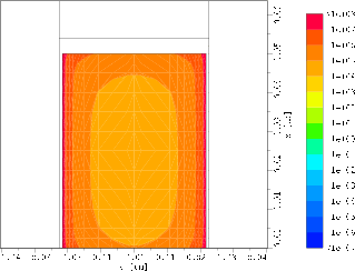
(a) Electron current density of the double-gate FinFET.
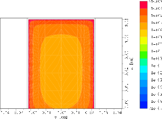
(b) Electron current density of the triple-gate FinFET. |
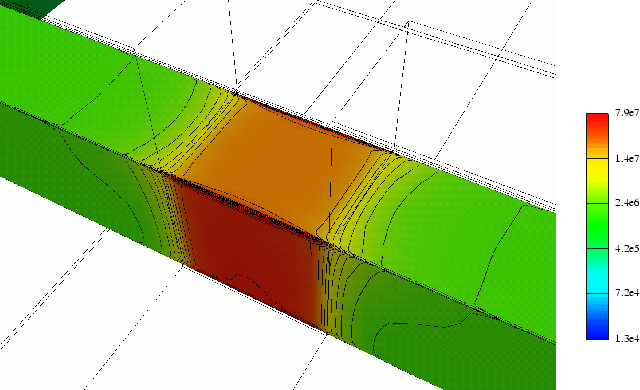
Fig. 4.28(a) and Fig. 4.28(b) show the vector component of the electron current density perpendicular to the cut for the double- and the triple-gate FinFET, respectively. One can clearly see the formation of the third channel on the top of the fin. Fig. 4.29 shows a three-dimensional view of the fin. A higher current density appears at the edges due to corner effects.
 |
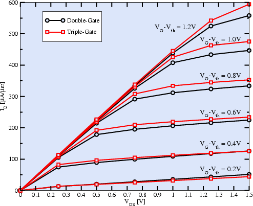
A comparison of the
![]() -
-
![]() characteristics of the
double-gate and the triple-gate FinFET is shown in
Fig. 4.30. The figure shows a small increasment of the
drive current due to the third gate.
characteristics of the
double-gate and the triple-gate FinFET is shown in
Fig. 4.30. The figure shows a small increasment of the
drive current due to the third gate.
Robert Klima 2003-02-06