4.3 Novel Implication Logic Gates Using STT-MTJs
4.3.1 Device Principles
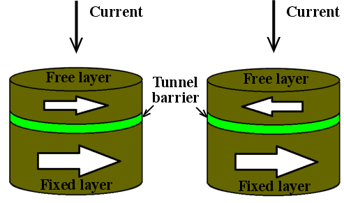
The basic structure of the magnetic tunnel junction consists of a free and a fixed (pinned) ferromagnetic layer
separated by a tunneling oxide (Fig. 4.8). The magnetization of the free layer has a bistable configuration
and can be switched between a parallel and an antiparallel state compared to the fixed magnetization
direction of the pinned layer. The MTJ exploits the tunnel magnetoresistance effect associated with the
relative angle between the magnetizations of the free and the pinned layers. An antiparallel alignment results
in a high-resistance state (HRS;  ) of the MTJ, while the parallel alignment places it in a low-resistance
state (LRS;
) of the MTJ, while the parallel alignment places it in a low-resistance
state (LRS;  ). The MTJ resistance modulation is described by the tunnel magnetoresistance
(TMR) ratio and is defined as
). The MTJ resistance modulation is described by the tunnel magnetoresistance
(TMR) ratio and is defined as 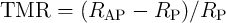 . Nowadays, the tunneling oxide is usually
MgO. Due to the enhanced spin filtering, MgO-based MTJs exhibit a high TMR ratio which
is facilitated to read-out the MTJ resistance state via the TMR effect [38]. The TMR ratio
record of up to 604% [182] reported in MgO-based MTJs is close to the theoretical maximum
(
. Nowadays, the tunneling oxide is usually
MgO. Due to the enhanced spin filtering, MgO-based MTJs exhibit a high TMR ratio which
is facilitated to read-out the MTJ resistance state via the TMR effect [38]. The TMR ratio
record of up to 604% [182] reported in MgO-based MTJs is close to the theoretical maximum
( 1000%) [183, 184].
The magnetic state of the MTJ free layer can be switched either by a magnetic field or by a spin-polarized
current via the STT effect. Compared to the first generation of MTJs, which utilized a magnetic field for
switching, the STT switching technique exhibits pure electrical read/write operations and renders the
current-carrying wire generating the magnetic field superfluous. This brings significant advantages with
respect to scalability and energy consumption [22]. It makes the STT-MTJ a suitable candidate for a
universal memory which combines the advantages of CMOS compatibility, non-volatility, high
switching speed, high integration density, unlimited endurance, and scalability. Furthermore, the
STT-MTJ shows memristive behavior [61, 71] as its magnetic state and thus the corresponding
resistance is a function of the historic profile of the current passing through the MTJ. Indeed, the
STT-MTJ exhibits the memristor fingerprint [71] characterized by a pinched  hysteresis
loop [185, 186].
hysteresis
loop [185, 186].
In the following, the STT-MTJ-based realization of the stateful implication logic operation is demonstrated
by using the conventional implication gate topology and a novel topology which significantly improves the
performance of the STT-MTJ-based implication logic gates (Fig. 4.12). In the STT-MTJ-based
logic gates, due to the magnetic bistability of the MTJ caused by an intrinsic damping in its
magnetic free layer [23], the magnetization of the free layer can relax to its initial state when
there is enough time (in the range of sub-nanosecond [187]) between sequential logic operations.
Therefore, unlike the TiO and the domain wall based logic gates, where the state drift errors
are accumulated as described before, the need for refreshing circuitry in the STT-MTJ-based
stateful logic systems is eliminated. In order to analyze and compare the performance of the
STT-MTJ-based logic gates, considerations regarding the reliability of these gates are explained in the next
section.
and the domain wall based logic gates, where the state drift errors
are accumulated as described before, the need for refreshing circuitry in the STT-MTJ-based
stateful logic systems is eliminated. In order to analyze and compare the performance of the
STT-MTJ-based logic gates, considerations regarding the reliability of these gates are explained in the next
section.
4.3.2 Reliability Modeling and Analysis
Initially, there was no performance analysis regarding STT-MTJ-based logic gates available, which are very
favorable for stateful logic applications as discussed before. However, as it is shown in the following, the
reliability analysis of the stateful logic operations is as an essential prerequisite for benchmarking and
performance comparison of different STT-MTJ-based logic architectures. Here, based on the
mechanism of the conditional switching behavior in stateful logic, a framework needed to perform
the reliability modeling and analysis for the STT-MTJ-based stateful logic gates is described
and used for investigating, optimizing, and comparing different STT-MTJ-based logic gates and
architectures.
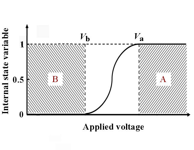
4.3.2.1. Reliable Switching
In order to analyze the stateful logic gates explained before and to further extend stateful logic to cover more
devices and circuit topologies, the conditional switching behavior of a memristive device can be
described by using Fig. 4.9, which shows the switching dynamic of a memristive element as a
function of the applied voltage/current pulse amplitude. The horizontal axis denotes the voltage (or
current) level applied to a memristive element for a specific time (a pulse duration of  ). The
solid curve indicates the high-to-low (or low-to-high) resistance switching behavior of the device
where the vertical axis represents a normalized internal state variable of the device. The internal
state variable can represent the deterministic switching model of the memristive device (e.g.
). The
solid curve indicates the high-to-low (or low-to-high) resistance switching behavior of the device
where the vertical axis represents a normalized internal state variable of the device. The internal
state variable can represent the deterministic switching model of the memristive device (e.g.
 in a TiO
 memristive switch or the relative domain wall position
  in a spintronic
memristor) or the switching probability of a spintronic memristive element with a stochastic switching
model (e.g.
in a spintronic
memristor) or the switching probability of a spintronic memristive element with a stochastic switching
model (e.g.  in a STT-MTJ). Region A shows a reliable switching region for which the
dashed line represents the minimum reliable switching voltage (
in a STT-MTJ). Region A shows a reliable switching region for which the
dashed line represents the minimum reliable switching voltage ( ) (or a corresponding current
 ). Region B denotes a reliable non-switching region for which the dashed line represents the
maximum reliable non-switching voltage (
). Region B denotes a reliable non-switching region for which the dashed line represents the
maximum reliable non-switching voltage ( ) below that the disturbance due to the applied
voltage/current is negligible and it cannot force a switching event. When
) below that the disturbance due to the applied
voltage/current is negligible and it cannot force a switching event. When  , the memristive device
has a nonzero switching voltage/current threshold which is in general a function of the pulse
duration
, the memristive device
has a nonzero switching voltage/current threshold which is in general a function of the pulse
duration  .
.
In the TiO or the DW-TMR memristive implication logic gates explained before, there are four possible
high-to-low resistance switching cases depending on the initial resistance states, when the voltage pulses
or the DW-TMR memristive implication logic gates explained before, there are four possible
high-to-low resistance switching cases depending on the initial resistance states, when the voltage pulses
 and
and  are applied to the gates. However, only when both
  and
and  are in the high resistance
state (State 1), the voltage drop on
are in the high resistance
state (State 1), the voltage drop on  (the current flowing through
  ) is higher than
  . In the other
cases, the voltage drops on
. In the other
cases, the voltage drops on  and
and  are below
  and, therefore, undesired switching events are avoided.
For example, as in State 3
and, therefore, undesired switching events are avoided.
For example, as in State 3  is in the low-resistance state, the voltage or current of
  is decreased and
thus its high-to-low resistance switching is avoided. This conditional switching behavior, which comprises a
set of desired and undesired switching events, corresponds to implication logic. Similarly, in a
STT-MTJ-based logic gate, depending on the initial resistance states of all MTJs a target (output)
MTJ is switched or not. Reliability of such a conditional switching behavior can be defined as a
function of the switching probabilities (
is decreased and
thus its high-to-low resistance switching is avoided. This conditional switching behavior, which comprises a
set of desired and undesired switching events, corresponds to implication logic. Similarly, in a
STT-MTJ-based logic gate, depending on the initial resistance states of all MTJs a target (output)
MTJ is switched or not. Reliability of such a conditional switching behavior can be defined as a
function of the switching probabilities ( ) of desired switching events as well as
  for
undesired switching events. This basic discussion can be used to study, optimize and compare
STT-MTJ-based logic gates. Furthermore, it provides a better understanding of the conditional
switching mechanism in stateful logic which paves the way for the proposal of logic gate with novel
topologies. In the following, a SPICE model of the STT-MTJs is presented and modified to have the
capability of calculating the reliabilities and error probabilities in the STT-MTJ-based logic
gates.
for
undesired switching events. This basic discussion can be used to study, optimize and compare
STT-MTJ-based logic gates. Furthermore, it provides a better understanding of the conditional
switching mechanism in stateful logic which paves the way for the proposal of logic gate with novel
topologies. In the following, a SPICE model of the STT-MTJs is presented and modified to have the
capability of calculating the reliabilities and error probabilities in the STT-MTJ-based logic
gates.
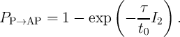
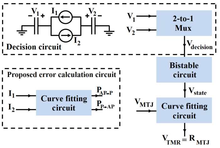
4.3.2.2. Modified STT-MTJ SPICE Model
The STT-MTJ SPICE model presented in [188] includes a (deterministic) decision circuit to control a
bistable circuit which shows an immediate switching between parallel and antiparallel states (Fig. 4.10). The
decision circuit comprises two capacitors (C and C
and C ) excited by two current sources (
 and
and  )
connected in parallel to realize the relationship between the critical switching time and the critical switching
current.
)
connected in parallel to realize the relationship between the critical switching time and the critical switching
current.
In fact, the rate of the charge/discharge of the capacitors is a function of the current flowing through the
MTJ ( ) and is determined by [188]
![( [ i ])
I1 = exp - Δ 1 - ------------
IC0(AP →P )](diss687x.png) | (4.10) |
and
![( [ ] )
-----i------
I2 = exp - Δ 1 - .
IC0 (P →AP )](diss688x.png) | (4.11) |
 is the thermal stability factor and is equal to
  .
.  represents the energy barrier between the
parallel and the antiparallel magnetization states of the MTJ,
represents the energy barrier between the
parallel and the antiparallel magnetization states of the MTJ,  is the Boltzmann constant, and
  is the
temperature.
is the
temperature.  and
and  denote the critical currents for the antiparallel-to-parallel
and parallel-to-antiparallel switching cases and are extrapolated to the critical switching time
denote the critical currents for the antiparallel-to-parallel
and parallel-to-antiparallel switching cases and are extrapolated to the critical switching time  ns. It
has been shown that the time required to charge the capacitors C
ns. It
has been shown that the time required to charge the capacitors C and C
and C by exactly 1 V with the
capacitance of 1 nF are given by [188]
by exactly 1 V with the
capacitance of 1 nF are given by [188]
![( [ ])
t = (1-nF--)(1-V-)-= 1 ns × exp Δ 1 - -----i------
C1 I1 IC0(AP →P )](diss699x.png) | (4.12) |
and
![( [ ] )
t = (1-nF--)(1-V-)-= 1 ns × exp Δ 1 - -----i------ .
C2 I2 IC0 (P →AP )](diss700x.png) | (4.13) |
In the thermally-activated switching regime (switching time  10 ns), Eq. 4.12 (Eq. 4.13) is identical to
the relationship between the critical switching time
10 ns), Eq. 4.12 (Eq. 4.13) is identical to
the relationship between the critical switching time  and the critical switching current (
 ) of
antiparallel-to-parallel (parallel-to-antiparallel) MTJ switching as [188]
) of
antiparallel-to-parallel (parallel-to-antiparallel) MTJ switching as [188]
![[ ]
tp-
IC = IC0 1 - Δ ln( ) .
t0](diss704x.png) | (4.14) |
As the critical values of switching time and current are usually defined for the MTJ switching probability of
50% [188], the decision circuit enforces an immediate switching to the bistable circuit as soon as the
switching probability is 50%. The curve fitting circuit is used to take the voltage-dependent effective TMR
ratio into account, which is important to determine the resistance-voltage characteristic of the MTJ. This
SPICE model covers the major electrical characteristics of the STT-MTJs. It is, however, not possible to
calculate the switching probabilities of the STT-MTJs required for reliability analysis and comparison of the
STT-MTJ-based logic gates only based on this SPICE model (Fig. 4.11). Therefore, in order to calculate the
STT-MTJ switching probability ( ), the theoretical expression for the thermally-activated switching
regime [189] is used
), the theoretical expression for the thermally-activated switching
regime [189] is used
![( [ ( ) ] )
τ IMTJ
Psw = 1 - exp - --exp - Δ 1 - ------ ,
t0 IC0](diss706x.png) | (4.15) |
where  is current flowing through the MTJ and
  is the pulse duration.
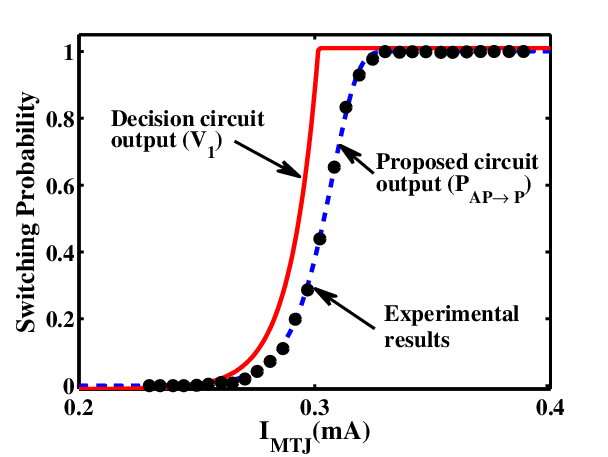
Eq. 4.15 has been experimentally verified in [49] and can be added to the STT-MTJ SPICE model for
switching probability (error) calculations by using a curve fitting circuit shown in Fig. 4.10 characterized
as
 | (4.16) |
and
 | (4.17) |
Fig. 4.11 compares the experimental results from [49] with the unmodified and the modified STT-MTJ
SPICE models. It illustrates that although the decision signals  in the (old) STT-MTJ SPICE predicts
the correct critical switching current where the probability of the switching is 50%, it cannot fit the
experimental data equally well.
in the (old) STT-MTJ SPICE predicts
the correct critical switching current where the probability of the switching is 50%, it cannot fit the
experimental data equally well.
In order to calculate the current flowing through the STT-MTJs in the stateful MTJ logic gates (described
later), the voltage-dependent effective TMR model [190] is used, which determines the resistance
characteristic of the MTJs in the antiparallel MTJ state as a function of the MTJ voltage ( )
as
)
as
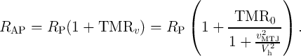 | (4.18) |
 and
and  are the TMR ratio under zero and non-zero bias voltage across the MTJ, respectively.
V
are the TMR ratio under zero and non-zero bias voltage across the MTJ, respectively.
V is the bias voltage equivalent to
 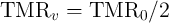 .
.
4.3.3 Improved Implication Logic Gate
As explained before, due to the magnetic bistability of the MTJ, STT-MTJ logic gates eliminate error
accumulation in stateful logic and thus are inherently suited for digital computing and are preferable over
TiO -based or domain wall-based technologies, which exhibit error accumulation due to their analog
behavior. In this section, STT-MTJs are employed to perform implication logic based on the conventional
voltage-controlled (VC) implication gate topology (Fig. 4.12a) and a novel current-controlled (CC) topology
(Fig. 4.12b). Based on the description of the reliable conditional switching cases (Section 4.3.2.1) and the
modified STT-MTJ model (Section 4.3.3), the performance of these gates are compared and it is
demonstrated that the proposed CC-IMP gate outperforms the conventional VC-IMP gate in terms of
reliability and power consumption.
-based or domain wall-based technologies, which exhibit error accumulation due to their analog
behavior. In this section, STT-MTJs are employed to perform implication logic based on the conventional
voltage-controlled (VC) implication gate topology (Fig. 4.12a) and a novel current-controlled (CC) topology
(Fig. 4.12b). Based on the description of the reliable conditional switching cases (Section 4.3.2.1) and the
modified STT-MTJ model (Section 4.3.3), the performance of these gates are compared and it is
demonstrated that the proposed CC-IMP gate outperforms the conventional VC-IMP gate in terms of
reliability and power consumption.
Similar to the memristive stateful implication gate (Table 3.2), in the voltage- and current-controlled
implication gates (Fig. 4.12a and Fig. 4.12b) the logic operation (N)IMP is realized based on a conditional
switching in the target MTJ ( ). Depending on the initial resistance states of the source and the
target MTJs, an AP–to–P STT switching event is enforced in the target MTJ only, when both
MTJs are initially at antiparallel (high resistance) states (State 1). For the other input patterns
(State 2, State 3, and State 4), the resistance states of the MTJs are left unchanged as shown in
Table 3.2. In the MTJ-based voltage-controlled implication (VC-IMP) gate (Fig. 4.12a), the logic
operation is executed by simultaneously applying the voltage pulses
). Depending on the initial resistance states of the source and the
target MTJs, an AP–to–P STT switching event is enforced in the target MTJ only, when both
MTJs are initially at antiparallel (high resistance) states (State 1). For the other input patterns
(State 2, State 3, and State 4), the resistance states of the MTJs are left unchanged as shown in
Table 3.2. In the MTJ-based voltage-controlled implication (VC-IMP) gate (Fig. 4.12a), the logic
operation is executed by simultaneously applying the voltage pulses  and
and  . As
. As
 , the voltage drop on
  is smaller than the critical voltage level required for
STT switching and thus
is smaller than the critical voltage level required for
STT switching and thus  is left unchanged. The resistance state of
  provides a voltage
modulation across
provides a voltage
modulation across  through
  . Due to this modulation,
  switches, when
  is in the
high resistance state (State 1), but remains unchanged, when
is in the
high resistance state (State 1), but remains unchanged, when  is in the low resistance state
(State 3).
is in the low resistance state
(State 3).
In the CC-IMP gate (Fig. 4.12b) the logic operation is performed by applying the current pulse  to the
gate.
to the
gate.  is applied in a direction which tends to enforce AP–to–P switching events to both
MTJs. The current
is applied in a direction which tends to enforce AP–to–P switching events to both
MTJs. The current  is split between
  and
and  inversely proportional to the total resistance
of each branch. The current split depends on the input pattern as the resistance value of each
branch is a function of the logic state of its MTJ. According to Table 3.2 there are four possible
AP–to–P switching events containing State 1 and State 3 for
inversely proportional to the total resistance
of each branch. The current split depends on the input pattern as the resistance value of each
branch is a function of the logic state of its MTJ. According to Table 3.2 there are four possible
AP–to–P switching events containing State 1 and State 3 for  and State 1 and State 2 for
 .
.
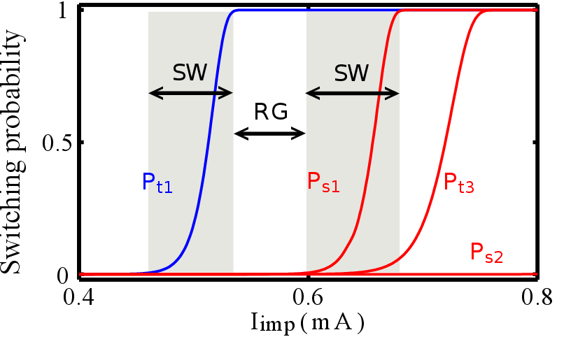
In order to better understand the operation of the implication gate, Fig. 4.13 shows the switching
probabilities of S ( ) and T (
 ) as a function of the current level applied to the implication gate (
 )
for all possible AP–to–P switching events
)
for all possible AP–to–P switching events  ,
,  ,
,  , and
, and  . The current direction of
  is fixed,
so that only high-to-low resistance switching is feasible in both MTJs for any input combination. When both
MTJs are initially in the high resistance state (State 1), low
is fixed,
so that only high-to-low resistance switching is feasible in both MTJs for any input combination. When both
MTJs are initially in the high resistance state (State 1), low  values (
 mA) can not enforce any
switching, because the currents flowing through both MTJs are below the required switching
current.
mA) can not enforce any
switching, because the currents flowing through both MTJs are below the required switching
current.
For a correct implication logic behavior,  (
( ) must (not) switch to the low resistance state. Thus,
  has to be chosen in a way that
  exhibits a high switching probability and
  remains unchanged
(within the reliable gap RG shown in Fig. 4.13). This gap is controlled by
remains unchanged
(within the reliable gap RG shown in Fig. 4.13). This gap is controlled by  as it limits the
current flow through
as it limits the
current flow through  . In State 2
  is in the high resistance state and the current flowing
through
is in the high resistance state and the current flowing
through  is lower than the value required for STT switching due to
  and the low resistance
state of
and the low resistance
state of  . In State 3, although
  is in the high resistance state,
  does not switch
  (
( ) since
  is in the low resistance state. This requires a high enough
  resistance
modulation (high TMR) and also restricts the upper limit for
resistance
modulation (high TMR) and also restricts the upper limit for  . When both MTJs are in the low
resistance state (State 4), there is no possible switching event as the direction of the
. When both MTJs are in the low
resistance state (State 4), there is no possible switching event as the direction of the  is
fixed.
is
fixed.
The reliability of the implication operation in State 1 is proportional to the multiplication of the
probability of the desired switching event in  (
( ) and the term
  , where
  is the
probability of the undesired switching event in
is the
probability of the undesired switching event in  . Therefore, in State 1, the error probability (
 )
is
)
is
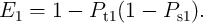 | (4.19) |
In State 2 and State 3, there are only undesired switching events ( and
and  ) in
) in  and
and  ,
respectively. Therefore, the error probabilities are given by
,
respectively. Therefore, the error probabilities are given by
 | (4.20) |
When both MTJs are in the low resistance state (State 4), there is no possible switching event and the error
probability  is zero. It is obvious that a reliable logic behavior of an operation is ensured only, when the
logic gate exhibits correct functionality for all input patterns. Therefore, by assuming equal incidence
probabilities for all input patterns, the average implication error probability (
is zero. It is obvious that a reliable logic behavior of an operation is ensured only, when the
logic gate exhibits correct functionality for all input patterns. Therefore, by assuming equal incidence
probabilities for all input patterns, the average implication error probability ( ) is obtained
by
) is obtained
by
 | (4.21) |
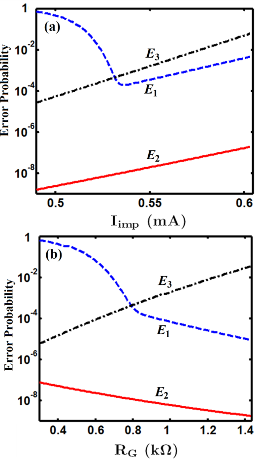
From a circuit point of view, the parameters ( and
and  in the CC-IMP and
  ,
,  , and
, and  in the VC-IMP gates) can be optimized to minimize the error probability
  for given MTJ device
characteristics. Fig. 4.14a shows the error probabilities
for given MTJ device
characteristics. Fig. 4.14a shows the error probabilities  for different input states of the CC-IMP gate as
function of
for different input states of the CC-IMP gate as
function of  for a fixed
  with MTJ devices characterized by
  ,
,  ,
,
 , and
, and  .
.  has to be high enough to enforce a desired
switching of
has to be high enough to enforce a desired
switching of  in State 1. However, there is an optimum
  , as increasing
  increases
the probabilities for undesired switching events in both
increases
the probabilities for undesired switching events in both  and
and  in State 1, State 2, and
State 3.
in State 1, State 2, and
State 3.
In the CC-IMP gate  provides a structural asymmetry which increases the current flowing through
  compared to
  , when both MTJs are in the high resistance state (State 1). Therefore, increasing
  reduces the error probability
  as it increases (decreases) the probability of the desired (undesired)
switching event
as it increases (decreases) the probability of the desired (undesired)
switching event  (
( ) as shown in Fig. 4.14b. However, its maximum value is limited by
  . In
State 3,
. In
State 3,  is in the low resistance state and thus the current flowing through
  is increased as compared to
State 1. Therefore, the current flowing through
is increased as compared to
State 1. Therefore, the current flowing through  is decreased to a lower level, below the critical current
required for the STT switching. Because a higher
is decreased to a lower level, below the critical current
required for the STT switching. Because a higher  decreases the effective resistance modulation of its
corresponding branch (the source branch comprises
decreases the effective resistance modulation of its
corresponding branch (the source branch comprises  and
and  ), it increases the error probability
  (Fig. 4.14b).
As explained before, a higher  reduces the error probabilities in State 1 and State 2 but is
limited by the required current modulation in State 3. The current modulation in State 3 relies
on the modulation of the MTJ resistance between its antiparallel and parallel magnetization
states described by the MTJ’s TMR ratio. From this follows that the TMR ratio is the main
device parameter affecting the reliability of the implication gate. A higher TMR ratio provides
a higher current modulation and allows higher values of
reduces the error probabilities in State 1 and State 2 but is
limited by the required current modulation in State 3. The current modulation in State 3 relies
on the modulation of the MTJ resistance between its antiparallel and parallel magnetization
states described by the MTJ’s TMR ratio. From this follows that the TMR ratio is the main
device parameter affecting the reliability of the implication gate. A higher TMR ratio provides
a higher current modulation and allows higher values of  for CC-IMP circuit parameters
optimization. Fig. 4.15a shows the two dominant error probabilities (
for CC-IMP circuit parameters
optimization. Fig. 4.15a shows the two dominant error probabilities ( and
and  ) for two
different TMR ratios. It illustrates that a higher TMR ratio has a negligible effect on
) for two
different TMR ratios. It illustrates that a higher TMR ratio has a negligible effect on  but it
decreases
but it
decreases  . Therefore, for MTJs with increased TMR, the CC-IMP gate with optimized circuit
parameters exhibits a more reliable logic behavior. In fact, as the current modulation between
State 1 and State 3 depends on the TMR ratio, a higher TMR ratio allows for higher values of
. Therefore, for MTJs with increased TMR, the CC-IMP gate with optimized circuit
parameters exhibits a more reliable logic behavior. In fact, as the current modulation between
State 1 and State 3 depends on the TMR ratio, a higher TMR ratio allows for higher values of
 (lower
  shown in Fig. 4.14b) when the circuit parameters are optimized. Fig. 4.15b
shows an example of a two-dimensional circuit parameters optimization for the CC-IMP logic
gate.
shown in Fig. 4.14b) when the circuit parameters are optimized. Fig. 4.15b
shows an example of a two-dimensional circuit parameters optimization for the CC-IMP logic
gate.
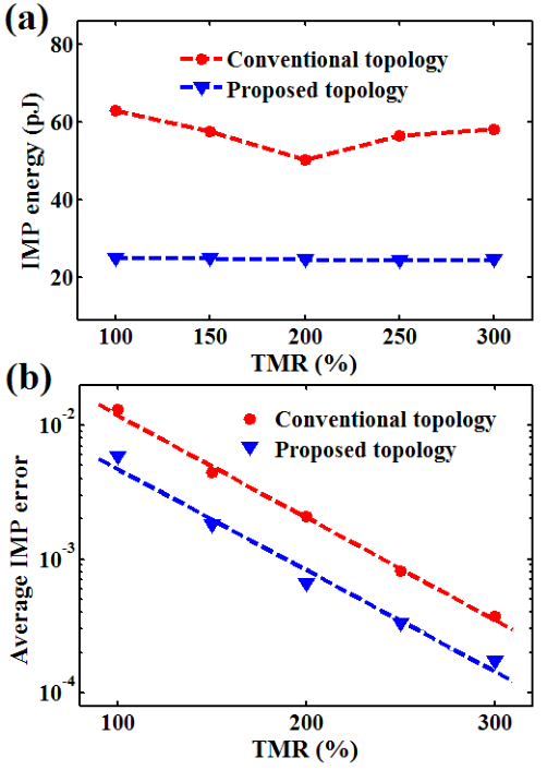
In order to compare the performance of the CC-IMP and VC-IMP gates, the circuit parameters are optimized
and the error probabilities and the energy consumptions are calculated. According to Fig. 4.16, the optimal
 of the implication gate based on the conventional topology (Fig. 4.12a) is higher by a factor of two to
three as compared to the proposed topology (Fig. 4.12b). Furthermore, in the conventional voltage-controlled
gate topology the current flowing through
of the implication gate based on the conventional topology (Fig. 4.12a) is higher by a factor of two to
three as compared to the proposed topology (Fig. 4.12b). Furthermore, in the conventional voltage-controlled
gate topology the current flowing through  is equal to the sum of the switching current
  and the
modulation current
and the
modulation current  (
( ) while it is only equal to the switching current
  in the novel
current-controlled gate topology (
in the novel
current-controlled gate topology ( ). Therefore, for a fixed current level and a given switching time,
the implication energy consumption is about 60% lower in the novel implication gate topology than in the
conventional topology. A comparison of the implication energy consumption in the two topologies is shown in
Fig. 4.17a.
). Therefore, for a fixed current level and a given switching time,
the implication energy consumption is about 60% lower in the novel implication gate topology than in the
conventional topology. A comparison of the implication energy consumption in the two topologies is shown in
Fig. 4.17a.
Robust implication logic behavior requires a high enough state dependent modulation in both topologies.
This modulation on the target MTJ ( ) which is caused by the difference between the high
and low resistances of the source MTJ (
) which is caused by the difference between the high
and low resistances of the source MTJ ( ), is directly proportional to the TMR ratio of the
MTJ. Therefore, from the device point of view, we expect that the error
), is directly proportional to the TMR ratio of the
MTJ. Therefore, from the device point of view, we expect that the error  decreases with
the increase of the TMR ratio which is a determinant device parameter for the logic reliability.
Fig. 4.17b demonstrates that the error
decreases with
the increase of the TMR ratio which is a determinant device parameter for the logic reliability.
Fig. 4.17b demonstrates that the error  decreases exponentially with increasing TMR ratio.
At a fixed TMR ratio the CC-IMP gate topology provides a higher modulation on
decreases exponentially with increasing TMR ratio.
At a fixed TMR ratio the CC-IMP gate topology provides a higher modulation on  , thus
reduces the average error probability by about 60% as compared to the conventional one. As the
proposed CC-IMP gate enables a more energy-efficient and reliable implementation for implication
logic framework, in the following we employ the CC-IMP gate for the performance comparison
between the STT-MTJ-based implication logic gates and the state-of-the-art (reprogrammable)
gates.
, thus
reduces the average error probability by about 60% as compared to the conventional one. As the
proposed CC-IMP gate enables a more energy-efficient and reliable implementation for implication
logic framework, in the following we employ the CC-IMP gate for the performance comparison
between the STT-MTJ-based implication logic gates and the state-of-the-art (reprogrammable)
gates.
 from the (unmodified) SPICE model.
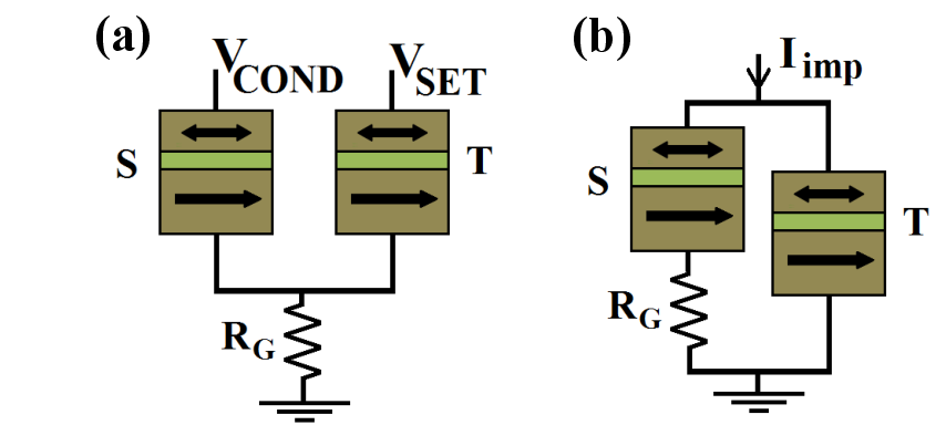
 and
and  in the CC-IMP gate as a function of
  .
.
 ) for different input states of the CC-IMP logic gate as function of (a)
  and
(b)
and
(b)  .
.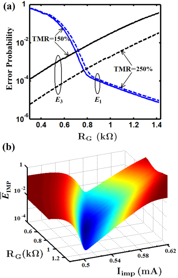
 and
and  ) for different TMR ratios. (b) Circuit parameters optimization
in the CC-IMP gate with TMR ratio and optimum
) for different TMR ratios. (b) Circuit parameters optimization
in the CC-IMP gate with TMR ratio and optimum  and
and  of
of  ,
,  , and
, and  , respectively.
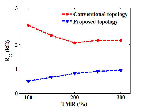
 in the conventional (VC-IMP) and the proposed (CC-IMP) implication logic gates depending
on the TMR ratio.
in the conventional (VC-IMP) and the proposed (CC-IMP) implication logic gates depending
on the TMR ratio.