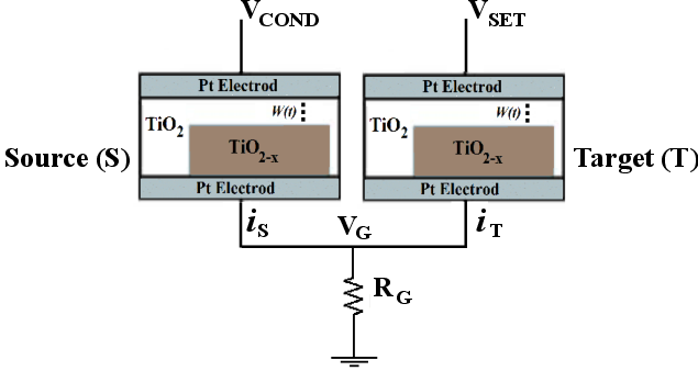
| Figure 3.2.: | Circuit topology of the TiO memristive implication logic gate. memristive implication logic gate. |
Recently, it has been shown that a fundamental Boolean logic operation called material implication (IMP) is
naturally realized in a simple circuit (Fig. 3.2) combining a conventional resistor and two TiO memristive
switches [75, 76]. This provides stateful logic where non-volatile memory devices are used as the computing
elements.
memristive
switches [75, 76]. This provides stateful logic where non-volatile memory devices are used as the computing
elements.
Material implication (IMP) is a fundamental two-input (e.g.  and
and  ) Boolean logic operation (
 ),
which reads ‘
),
which reads ‘ implies
  ’ or ‘if
  , then
  ’, and is equivalent to ‘(NOT
  ) OR
) OR  ’ (
’ ( ) as
shown in Table 3.1. The symbols
) as
shown in Table 3.1. The symbols  and
and  are chosen as they represent the logic states of a
source (S) and a target (T) memory element in the stateful logic gate. The operations IMP and
NIMP (negated IMP) form a computationally complete logic basis in combination with any
operation from the sets C and
are chosen as they represent the logic states of a
source (S) and a target (T) memory element in the stateful logic gate. The operations IMP and
NIMP (negated IMP) form a computationally complete logic basis in combination with any
operation from the sets C and  , respectively, for which
  and
and
 and are therefore able to compute arbitrary Boolean
functions.
and are therefore able to compute arbitrary Boolean
functions.
Besides the AND, OR, and NOT operations, the IMP operation has been classified by Whitehead and Russell as one of the four basic logic operations in 1910 [160]. However, by modeling Boolean logic with circuits built with relays and switches, Shannon founded modern digital electronics [161] only based on AND, OR, and NOT operations due to their straightforward implementation. Since then, the IMP operation has been ignored in digital electronics. Only recently, it was demonstrated that memristive switches intrinsically enable the IMP operation in a crossbar array [75].
| Table 3.1.: | Truth tables of the basic implication operations, IMP and NIMP (negated IMP). |
| State | s t | s  t t |  |
| 1 | 0 0 | 1 | 0 |
| 2 | 0 1 | 1 | 1 |
| 3 | 1 0 | 0 | 0 |
| 4 | 1 1 | 1 | 0 |
| Table 3.2.: | Realized conditional switching behavior is equivalent to the operation IMP or NIMP depending on the definitions for the high and low resistance states (HRS and LRS) as logical ‘0’ and ‘1’. |
|
Implication operation |
HRS  0, LRS 0, LRS 1 1 |
HRS  1, LRS 1, LRS 0 0 | |||||
|
(conditional switching) |
t   | t   | |||||
State | s t | s t t | s t | t | s t | t |
|
| 1 | HRS HRS | HRS LRS | 0 0 | 1 | 1 1 | 0 | |
| 2 | HRS LRS | HRS LRS | 0 1 | 1 | 1 0 | 0 | |
| 3 | LRS HRS | LRS HRS | 1 0 | 0 | 0 1 | 1 | |
| 4 | LRS LRS | LRS LRS | 1 1 | 1 | 0 0 | 0 | |
Fig. 3.2 shows the circuit topology of the TiO memristive implication logic gate [75] combining two TiO
 memristors,
  and
and  , with a conventional resistor
  . The initial resistance states of the source (
 ) and
target (
) and
target ( ) memristors (denoted by the logic variable
  and
and  , respectively) are the logic inputs
of the gate. The final resistance state of
, respectively) are the logic inputs
of the gate. The final resistance state of  after performing the logic operation (
 ) is the
logic output of the gate. Performing the logic operation (
) is the
logic output of the gate. Performing the logic operation ( ) involves simultaneous
application of two negative voltage pulses,
) involves simultaneous
application of two negative voltage pulses,  and
and  , to the non-common terminals of
  and
and  .
.  is a negative voltage with smaller amplitude than
  (
( ).
Therefore, the voltage drop on
).
Therefore, the voltage drop on  is smaller than
  (the voltage level required for memristor
high-to-low resistance switching) and it remains unchanged after the operation for any input
patterns. However, depending on the resistance state of
(the voltage level required for memristor
high-to-low resistance switching) and it remains unchanged after the operation for any input
patterns. However, depending on the resistance state of  , the voltage
  changes the
voltage level on the common terminal of
changes the
voltage level on the common terminal of  and
and  (
( ) and modulates the voltage drop on the
target memristor
) and modulates the voltage drop on the
target memristor  . This provides a conditional switching behavior in
  , which is shown in
Table 3.2. In fact, the negative voltage pulse
, which is shown in
Table 3.2. In fact, the negative voltage pulse  enforces a high-to-low resistance switching of
 only, when both memristors are initially in the high resistance state (State 1). The voltage
 has a higher amplitude compared to
  as it must compensate the voltage drop on
 .
.
According to Table 3.2, depending on the logical definitions for the memristor low (LRS) and high (HRS)
resistance states, LRS  logic ‘1’ and HRS
  logic ‘0’ or vice-versa, the realized conditional switching
behavior is corresponding to the IMP or NIMP (negated IMP) operation (Table 3.1). In accordance with the
convention of Shannon, if we define HRS
logic ‘0’ or vice-versa, the realized conditional switching
behavior is corresponding to the IMP or NIMP (negated IMP) operation (Table 3.1). In accordance with the
convention of Shannon, if we define HRS  1 and LRS
  0, the logic output of the implication gate
corresponds to the NIMP operation as
0, the logic output of the implication gate
corresponds to the NIMP operation as
| {t′ = t NIMP s}≡t → s ≡{t′ = t.s = t AND ss}, | (3.1) |
 is the final state of the variable
  after the operation. In combination with the low-to-high
resistance switching, which corresponds to the TRUE operation (writing logic ‘1’) according to the above
definition, the NIMP operation forms a complete logic basis to compute any Boolean function. Therefore, it
enables stateful logic operations by memristive devices used simultaneously as non-volatile memory and logic
gates [75]. For instance, stateful universal NOR and NAND operations can be performed in three and five
sequential steps as Eq. 3.2 and Eq. 3.3, respectively.
Here,
after the operation. In combination with the low-to-high
resistance switching, which corresponds to the TRUE operation (writing logic ‘1’) according to the above
definition, the NIMP operation forms a complete logic basis to compute any Boolean function. Therefore, it
enables stateful logic operations by memristive devices used simultaneously as non-volatile memory and logic
gates [75]. For instance, stateful universal NOR and NAND operations can be performed in three and five
sequential steps as Eq. 3.2 and Eq. 3.3, respectively.
Here,  (
( ) represents the initial (final) logic variable equivalent to the resistance state of a third
memristor storing the logic result of intermediary logic steps and the final result of stateful NAND and NOR
operations. It should be noted that each logic variable (e.g.
) represents the initial (final) logic variable equivalent to the resistance state of a third
memristor storing the logic result of intermediary logic steps and the final result of stateful NAND and NOR
operations. It should be noted that each logic variable (e.g.  ) used as an input in Step
  is equal to the
final logic value (
is equal to the
final logic value ( ) from the previous step (Step
  ) since it has been directly stored in a non-volatile
memory element (A).
) since it has been directly stored in a non-volatile
memory element (A).