4.2 Implication Logic Using DW-TMR Memristors
Combining the domain wall (DW) motion induced by the spin-transfer torque (STT) [44, 45] with the
tunnel magnetoresistance (TMR) effect [169] has launched new concepts for spintronic memristive
devices [61, 96, 64]. The TMR effect is observed as a change in the electrical resistance of a magnetic
device depending on the relative magnetization states of two ferromagnetic layers separated by a
non-magnetic insulating layer (whether ferromagnetic layers are in a parallel or an antiparallel
alignment). Compared to the memristive devices based on ionic motion (e.g. TiO memristor),
spintronic memristors are more favorable in terms of speed, endurance, fine-tunability, and CMOS
compatibility [136, 65, 116, 81]. In this section it is shown that the implication logic operation can be
implemented based on DW-TMR memristive devices (Fig. 4.2), with the DW positions serving as
state variables. This enables stateful logic operations that extends spintronics from non-volatile
memory to logic applications, for which the spintronic memristor serves simultaneously as gate and
latch.
memristor),
spintronic memristors are more favorable in terms of speed, endurance, fine-tunability, and CMOS
compatibility [136, 65, 116, 81]. In this section it is shown that the implication logic operation can be
implemented based on DW-TMR memristive devices (Fig. 4.2), with the DW positions serving as
state variables. This enables stateful logic operations that extends spintronics from non-volatile
memory to logic applications, for which the spintronic memristor serves simultaneously as gate and
latch.
4.2.1 DW-TMR Memristor
The STT effect allows to manipulate the local magnetization in a magnetic device by transfusion
of magnetic momentum from a spin polarized current. Therefore, a spin-polarized current can
induce motion in magnetic domain walls. Because of its potential applications, STT domain wall
motion (STT-DWM) has generated wide interest and has been well studied theoretically and
experimentally [170, 171, 172, 173, 174, 175, 176, 177]. In a spintronic device, when the total electrical
resistance depends on the magnetization state, on one hand, and the current flowing through the
device can modulate the magnetization state, on the other hand, the device exhibits memristive
capabilities [60, 61, 62, 63, 64, 65, 66, 67]. In fact, the magnetization state and thus the electrical
resistance of such a device becomes a function of the historic profile of the current or the voltage applied to
the device which represents memristive behavior.
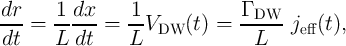
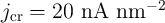
Fig. 4.2 shows the basic structure[96, 137] and a (possible) top view [64] of a domain wall tunnel
magnetoresistance (DW-TMR) memristor comprising an insulating layer and two ferromagnetic layers, a
reference layer with a fixed (pinned) magnetization state and a free layer which is divided into two segments
by a magnetic domain wall. The electrical resistance of the device depends on the relative orientation of the
magnetization directions. A complete antiparallel alignment results in a high-resistance state (HRS;  ) of
the device, while a fully parallel alignment places it in a low-resistance state (LRS;
) of
the device, while a fully parallel alignment places it in a low-resistance state (LRS;  ). The total resistance
(memristance) of the device is modeled by two resistors connected in parallel
). The total resistance
(memristance) of the device is modeled by two resistors connected in parallel  and
and  as [137]
 | (4.1) |
and
 | (4.2) |
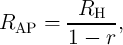
where  is the domain wall position,
  represent the relative DW position (
 ), and
  denotes the length of the free layer. Therefore, the
  characteristics of the device is obtained
as
characteristics of the device is obtained
as
 | (4.3) |
where
 | (4.4) |
When the DW velocity  is proportional to the applied current density (
 ), the dynamics
of
), the dynamics
of  is obtained as [137]
 | (4.5) |
where
 | (4.6) |
 is a DW velocity coefficient related to the device characteristics and
  is the DW cross-sectional
surface. The DWM appears when the current density
is the DW cross-sectional
surface. The DWM appears when the current density  is above a critical current density (
 ) [137].
Eq. 4.4 and Eq. 4.5 demonstrate that the device acts as a memristive system. Recently, a physical realization
of DW-TMR memristive devices has been reported in [64].
) [137].
Eq. 4.4 and Eq. 4.5 demonstrate that the device acts as a memristive system. Recently, a physical realization
of DW-TMR memristive devices has been reported in [64].
4.2.2 Domain Wall Dynamics
The DW-TMR memristor model described above includes simplifying assumption from [137] regarding the
dynamics of the current-induced DWM ( ). Here, a more accurate modeling of the current-induced
DWM is presented which can be used to drive the State equation (Eq. 2.15) of the DW-based devices
operating as memristive systems (see Section 2.1.2).
). Here, a more accurate modeling of the current-induced
DWM is presented which can be used to drive the State equation (Eq. 2.15) of the DW-based devices
operating as memristive systems (see Section 2.1.2).
The modified Landau-Lifshitz-Gilbert (LLG) equation [178] with an added spin-torque term [45] can be used
to describe the magnetization dynamics of a current-induced DWM as [174, 175]
 = -γ0 = -γ0 × × eff + α eff + α × × - - ![[ ( ) ]
⃗ ⃗
(⃗u. ∇ )⃗m - β ⃗m × (⃗u. ∇ )⃗m](diss522x.png) . . | | (4.7) |
 is a unit vector representing the direction of the local magnetic moments,
  is the gyromagnetic
ratio,
is the gyromagnetic
ratio,  denotes the effective magnetic field,
  represents the Gilbert damping parameter. The third
term in Eq. 4.7 represents the spin-torque term of the current flowing in the direction
represents the Gilbert damping parameter. The third
term in Eq. 4.7 represents the spin-torque term of the current flowing in the direction  , where
  shows
the injected current density,
shows
the injected current density,  denotes the spin polarization of the current,
  is the Bohr magneton,
 represents the saturation magnetization, and
  defines the strength of the non-adiabatic
spin-torque.
defines the strength of the non-adiabatic
spin-torque.
By using the collective coordinate approach which assumes that the configuration of the DW can be
explained by the collective coordinates the DW position ( ) and the angle between spins at the wall center
and the easy plane (
) and the angle between spins at the wall center
and the easy plane ( ), the LLG is simplified to Eq. 4.8 [179, 180].
|  + α + α = β ĵ, = β ĵ, | (4.8a)
|
|  - α - α = sin(2ϕ) + ĵ, = sin(2ϕ) + ĵ, | (4.8b) |
where  ,
,  ,
,  , represent the aspect parameters time, DW position, and
current density which are normalized to dimensionless units. Here,
, represent the aspect parameters time, DW position, and
current density which are normalized to dimensionless units. Here, 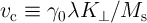 is a constant with the
velocity dimension,
is a constant with the
velocity dimension,  is the DW thickness,
  is the hard-axis anisotropy,
  is exchange
coupling constant, and
is exchange
coupling constant, and  denotes the easy-axis anisotropy.
4.2.3 DW-TMR-Based Implication Logic
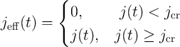
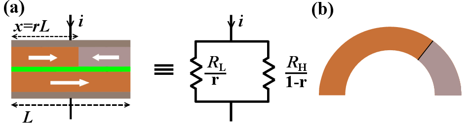
Fig. 4.3 shows an implication logic gate exploiting the DW-TMR memristive devices as non-volatile memory
as well as logic gates. The implication operation is performed by applying the voltage pulses  and
and
 which tend to enforce high-to-low resistance switching in the memristive device
  and
and
 .
.
The electrical resistances of  and
and  depend on the position of their DWs
  and
and  which act as the
state variables. The realization of the implication logic operating relies on a threshold current density below
that the DWs does not move. Similar to the TiO
which act as the
state variables. The realization of the implication logic operating relies on a threshold current density below
that the DWs does not move. Similar to the TiO -based implication logic gate, a high-to-low
resistance switching is enforced in the target device (
-based implication logic gate, a high-to-low
resistance switching is enforced in the target device ( ) only when both
  and
and  are in
the high resistance state (State 1 shown in Table 3.2). Therefore, the conditional switching
behavior equivalent to the basic operation of the implication logic is feasible using DW-TMR
memristors.
are in
the high resistance state (State 1 shown in Table 3.2). Therefore, the conditional switching
behavior equivalent to the basic operation of the implication logic is feasible using DW-TMR
memristors.
In order to analyze the DW-TMR-based implication logic gate (Fig. 4.3), Eq. 4.4–Eq. 4.6 are numerically
solved for both  and
and  coupled with Eq. 3.4 where
  and
and  are the currents following through
  and
and  , respectively.
  and
and  represent their memristances which are a function of
  and
and
 , respectively.
4.2.4 Simulation Results and Discussion
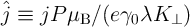
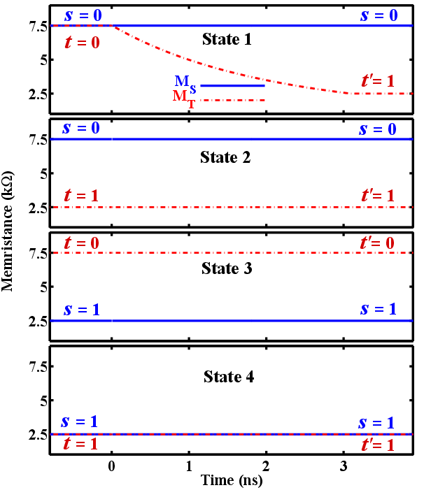
When  and
and  are in the high-resistance state (State 1), the current passing through
  (
( ) is above
the critical current
) is above
the critical current  required for the STT-DWM (Fig. 4.4). Due to the voltage drop on
  , the current
passing through
, the current
passing through  (
( ) is below
  and thus its DW does not move. Therefore, a high-to-low resistance
switching is enforced only in
and thus its DW does not move. Therefore, a high-to-low resistance
switching is enforced only in  and
and  is left unchanged (State 1 in Fig. 4.5). As during the switching
 decreases, the current density
  (
( ) is increased (decreased). This acts as a positive feedback
between
) is increased (decreased). This acts as a positive feedback
between  and
and  which accelerates the current-induced DWM and allows reducing the time
required for the implication operation. The memristor devices are characterized in [137] with
physical dimensions and electrical parameters assumed as: the length of
which accelerates the current-induced DWM and allows reducing the time
required for the implication operation. The memristor devices are characterized in [137] with
physical dimensions and electrical parameters assumed as: the length of  nm, the width of
 nm, the thickness of
  nm,
nm,  ,
,  ,
,  , and
, and
 .
.
The resistance states of S and  are left unchanged for other combinations of initial states (State 2 –
State 4 shown in Fig. 4.5). In fact, their current densities are below
are left unchanged for other combinations of initial states (State 2 –
State 4 shown in Fig. 4.5). In fact, their current densities are below  when they are initially in
the high resistance state (
when they are initially in
the high resistance state ( in State 2 and
  in State 3 shown in Fig. 4.4). Therefore,
the DW-TMR memristive gate exhibits the conditional switching behavior shown in Table 3.2.
This is equivalent to the basic operation of the implication logic and enables spintronic stateful
logic.
in State 3 shown in Fig. 4.4). Therefore,
the DW-TMR memristive gate exhibits the conditional switching behavior shown in Table 3.2.
This is equivalent to the basic operation of the implication logic and enables spintronic stateful
logic.
Fig. 4.6 shows the energy consumption of the DW-TMR gate ( ) at different initial states (State
  ) as a
function of
) as a
function of 
![∫ τimp
E = [M i2+ M i2 + R (i + i )2]dt,
i S S T T G S T
0](diss611x.png) | (4.9) |
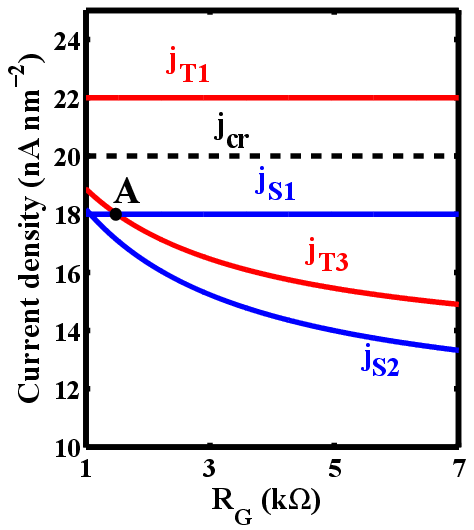
According to Fig. 4.6, a higher  increases the implication energy consumption. However, its minimum
value is limited by State 3 to provide a correct logic behavior as shown in Fig. 4.4. In fact, a higher
increases the implication energy consumption. However, its minimum
value is limited by State 3 to provide a correct logic behavior as shown in Fig. 4.4. In fact, a higher  increases the difference between
  and
and  and ensures that
  is not switched in State 3. Therefore,
Point A for which
is not switched in State 3. Therefore,
Point A for which  (shown in Fig. 4.4) indicates an optimum value of
  to ensure the correct
logic behavior in all states.
to ensure the correct
logic behavior in all states.
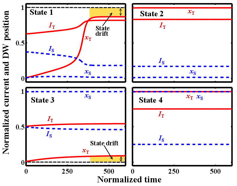
For more accurate analysis regarding the state drift errors, the one-dimensional model of magnetic DWs
(see Section 4.2.2) has been used to investigate the DW dynamics in  and
and  during the
implication operation. Here, coupled with Eq. 4.4 for
during the
implication operation. Here, coupled with Eq. 4.4 for  and
and  , Eq. 3.4 is numerically solved to
calculate
, Eq. 3.4 is numerically solved to
calculate  (
( ) as a function of
  (
( ), while the dynamics of
  (
( ) is obtained by
using Eq. 4.8. The memristor device geometries are supposed as
) is obtained by
using Eq. 4.8. The memristor device geometries are supposed as  ,
,  , and the
free layer thickness as
, and the
free layer thickness as  . Fig. 4.7 shows the DW dynamics of
  and T for all possible
inputs (State 1 to State 4). Due to their polarities, the voltage pulses
and T for all possible
inputs (State 1 to State 4). Due to their polarities, the voltage pulses  and
and  tend to
increase
tend to
increase  and
and  to enforce parallel alignment between free and pinned layers of
  and
and
 .
.
Since, the structure of the DW-TMR memristor devices is based upon existing magnetic memory technology
it combines the advantages of CMOS compatibility, high speed, high density, almost unlimited endurance,
and scalability and thus is very promising for spintronic memristors implementation [64]. However, although
in stateful implication logic the DW-TMR memristors are used as two-resistance-state devices, they exhibits
analog behavior as the DW displacement is continuous in value and is proportional to the amplitude of the
injected current and the pulse duration. Therefore, similar to the TiO -based logic gates, this causes a
state drift error during the implication operation. This error accumulates in sequential logic
steps and is very unfavorable for stateful logic as it results in a computation error after a certain
number of logic steps. According to Fig. 4.7, the major state drift error happens in
-based logic gates, this causes a
state drift error during the implication operation. This error accumulates in sequential logic
steps and is very unfavorable for stateful logic as it results in a computation error after a certain
number of logic steps. According to Fig. 4.7, the major state drift error happens in  . It
illustrates that after one implication operation the state drift error is about 10% and 5% in State 1
and State 3, respectively. Therefore, a refreshing is required after less than 10 logic steps as an
accumulated error of
. It
illustrates that after one implication operation the state drift error is about 10% and 5% in State 1
and State 3, respectively. Therefore, a refreshing is required after less than 10 logic steps as an
accumulated error of  cause a one-bit error in the readout. In the next section the realization of
implication logic using STT-MTJs is demonstrated, which does not suffer from error accumulation
problems. It is based on the STT-MRAM technology which has recently been commercialized by
Everspin [181].
cause a one-bit error in the readout. In the next section the realization of
implication logic using STT-MTJs is demonstrated, which does not suffer from error accumulation
problems. It is based on the STT-MRAM technology which has recently been commercialized by
Everspin [181].
 and
and  as a function of
  .
.
 and
and  during the implication operation for different initial logic states (State 1 – State 4) explained
in Table
during the implication operation for different initial logic states (State 1 – State 4) explained
in Table 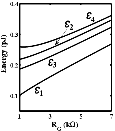
 ) as a function of
  in State
  .
.
 and
and  ) and the DW position ratios (
 and
and  ) of
) of  and
and  during the
implication operation.
during the
implication operation.