5.1 Overview
In Chapter 4 it has been described how the direct communication between STT-MTJs via implication and
reprogrammable circuit topologies realizes stateful logic operations. This intrinsically enables logic-in-memory
architectures and extends the functionality of non-volatile memory circuits to incorporate logic computations.
Nevertheless, in order to generalize the MTJ-based logic gates to large-scale logic circuits for performing more
complex logic functions, there are some issues which need to be addressed. For example, it is necessary to use
the logic result of one implication or reprogrammable gate as the input for the next logic stage (non-volatile
logic fan-out). However, as shown in Fig. 4.12 and Fig. 4.18, the input and the output MTJs are
physically connected to each other and any additional connection to other MTJs will disturb
the conditional switching behavior of the output (target) MTJ. This highly localizes the logic
computations and limits the possibility of performing logic operations between different inputs
located in arbitrary parts of the logic circuits. Therefore, intermediate circuitry is required to
perform extra read/write operations to readout the data stored in the output (target) MTJ
and to write it to an input (source) MTJ, which increases complexity, energy consumption, and
delay.
In the current-controlled implication circuit topology (Fig. 4.12b), the target MTJ cannot be used as a
source MTJ for the next logic stage due to a structural asymmetry caused by the resistor  . In the
reprogrammable circuit topologies (Fig. 4.18), the output MTJ cannot be used as an input MTJ as its
parallel connection to other MTJs limits the possibility to perform the conditional switching required for
MTJ-based logic. Furthermore, in order to cover all logic input patterns, independent access to
initialize all input MTJs is necessary. Therefore, magnetic-field-based switching is used for the input
MTJs [55]. This requires extra wiring for generating a current-induced Oersted field and thus in
contrast to STT-switching is prohibitive from both scalability and energy consumption points of
view [22].
. In the
reprogrammable circuit topologies (Fig. 4.18), the output MTJ cannot be used as an input MTJ as its
parallel connection to other MTJs limits the possibility to perform the conditional switching required for
MTJ-based logic. Furthermore, in order to cover all logic input patterns, independent access to
initialize all input MTJs is necessary. Therefore, magnetic-field-based switching is used for the input
MTJs [55]. This requires extra wiring for generating a current-induced Oersted field and thus in
contrast to STT-switching is prohibitive from both scalability and energy consumption points of
view [22].
Due to the easy integration of MTJs on top of a CMOS circuit into a one-transistor/one-MTJ (1T/1MTJ)
cell, hybrid CMOS/MTJ technology is promising to address the above mentioned issues for extending the
MTJ logic gates to large-scale non-volatile circuits. Since the 1T/1MTJ cell is the basic memory cell in the
STT-MRAM structure [49, 39], a STT-MRAM array can be used as a magnetic logic circuit for the
development of innovative non-volatile large-scale logic architectures. STT-MRAM combines the speed of
static RAM (SRAM), the density of dynamic RAM (DRAM), the non-volatility of flash memory, and has all
the characteristics of a universal memory [39]. In this chapter, it is shown how the MTJ reprogrammable
and implication stateful logic gates can be generalized to large-scale logic systems based on the
STT-MRAM arrays. This enables the extension of non-volatile MRAM from memory to logic computing
applications and eliminates the need for sensing amplifiers and intermediate circuitry [168] as
compared to the MTJ logic presented before as well as other hybrid CMOS/MTJ non-volatile logic
proposals [192].
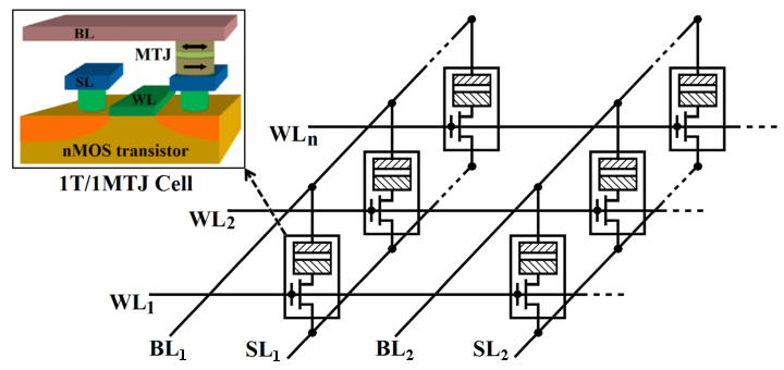
In the common STT-MRAM architecture (Fig. 5.1), the 1T/1MTJ cell contains one MTJ to store the binary
data and an access transistor to control the current flowing through the MTJ [49]. The cells are coupled in
parallel between the current-carrying source lines (SLs) and bit lines (BLs) as shown in Fig. 5.1.
The gate terminals of the access transistors are coupled to the word lines (WLs) in order to
apply proper voltage signals to a specific MTJ for read/write operations (memory mode) through
the SL and the BL in the MRAM array. For the read operation, a select voltage and a read
current are applied to the specific WL and BL. The reading current flows through the selected
MTJ, and by sensing the generated voltage difference between the SL and the BL, the resistance
(logic) state of the selected MTJ is sensed. The read current must be low enough to prevent an
undesired switching, which is referred to as a read disturbance. During a write operation, a select
voltage and a write current (voltage) are applied to the specific WL and BL. According to the
polarity of the current (voltage) applied to the current-carrying lines (SL and BL), the AP–to–P
or P–to–AP switching is enforced in the selected MTJ depending on the desired binary states
(logical ‘0’ or ‘1’). In the following it is shown how STT-MRAM arrays can be combined to
realize MTJ logic gates without the need for intermediate circuitry and independent CMOS logic
units.