3.3 Modeling
As explained before, by applying the voltage pulses  and
and  , a (desired) high-to-low resistance
switching (shown in bold in Table 3.2) is enforced in
, a (desired) high-to-low resistance
switching (shown in bold in Table 3.2) is enforced in  only in State 1. However, the current flowing
through the memristors tends to decrease their electrical resistances and change the internal state variable
only in State 1. However, the current flowing
through the memristors tends to decrease their electrical resistances and change the internal state variable
 . This phenomenon is called “state drift” (SD) [162] and its accumulation after a specific number of
sequential (N)IMP operations causes an undesired switching event (computation error) either in
. This phenomenon is called “state drift” (SD) [162] and its accumulation after a specific number of
sequential (N)IMP operations causes an undesired switching event (computation error) either in
 or
or  . This is due to the fact that, although the TiO
 memristive switches are used as
two-resistance-state devices for binary data storage, they actually act as analog elements since
the parameter
memristive switches are used as
two-resistance-state devices for binary data storage, they actually act as analog elements since
the parameter  changes continuously [142]. The design procedure of the IMP gate involves
determining the proper values of the circuit parameters (
changes continuously [142]. The design procedure of the IMP gate involves
determining the proper values of the circuit parameters ( ,
,  and
and  ) to minimize the
SD errors (SDEs). The design procedure presented in [162], which is the only existing design
procedure to the author’s knowledge, is based on a linear ionic drift model for the TiO
) to minimize the
SD errors (SDEs). The design procedure presented in [162], which is the only existing design
procedure to the author’s knowledge, is based on a linear ionic drift model for the TiO memristive
devices described below. However, as it is shown in the following, a more accurate model of
the TiO
memristive
devices described below. However, as it is shown in the following, a more accurate model of
the TiO memristive device has to be employed to analysis and optimize the stateful logic
gates.
memristive device has to be employed to analysis and optimize the stateful logic
gates.
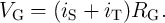
According to Fig. 3.2, the voltage drops on  and
and  are given by
| vS | = V COND - V G = iSMS | (3.4a)
|
| vT | = V SET - V G = iTMT, | (3.4b) |
where
 | (3.5) |
 denotes the voltage drop on
  and
and  (
( ) and
) and  (
( ) are the current and the memristances
of the memristive devices
) are the current and the memristances
of the memristive devices  (
( ), respectively. As, in general, the memristance is a nonlinear resistance
which depends on the historic profile of the current (voltage) applied to the memristor,
), respectively. As, in general, the memristance is a nonlinear resistance
which depends on the historic profile of the current (voltage) applied to the memristor,  and
and  are a
function of
are a
function of  (
( ) and
) and  (
( ) as well as their initial resistance states (the logic input
pattern). Therefore, in order to optimize the implication gate and to investigate the switching
behavior of
) as well as their initial resistance states (the logic input
pattern). Therefore, in order to optimize the implication gate and to investigate the switching
behavior of  and
and  , one has to solve Eq. 3.4 coupled with an appropriate memristor device
model which accurately describes the
, one has to solve Eq. 3.4 coupled with an appropriate memristor device
model which accurately describes the  characteristics of
  and
and  . In the following,
two TiO
. In the following,
two TiO memristor device models and simulation studies obtained from these models are
presented.
memristor device models and simulation studies obtained from these models are
presented.
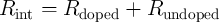
Fig. 3.3 shows a schematic of the TiO memristor structure containing a sandwiched TiO
 thin film and
two platinum (Pt) electrodes. During an electroforming process, as dopant acting oxygen vacancies are
created in the TiO
thin film and
two platinum (Pt) electrodes. During an electroforming process, as dopant acting oxygen vacancies are
created in the TiO thin-film except a narrow tunnel barrier of
  [138]. Therefore, the thin
film is divided into a (high conducting) doped region and an (insulating) undoped region and
its total resistance (internal resistance) is equal to the sum of the variable resistances on each
region:
[138]. Therefore, the thin
film is divided into a (high conducting) doped region and an (insulating) undoped region and
its total resistance (internal resistance) is equal to the sum of the variable resistances on each
region:
 | (3.6) |
The resistance switching mechanism of the device is related to the drift motion of dopants (oxygen vacancies)
due to an electric field across the device[114]. Therefore, this device shows memristive behavior as the width
of the undoped region ( in Fig. 3.3) and thus the total electrical resistance of the device depends on the
historic profile of the applied voltage/current to the device. According to the mathematical definition
of a memristive system (Eq. 2.14),
in Fig. 3.3) and thus the total electrical resistance of the device depends on the
historic profile of the applied voltage/current to the device. According to the mathematical definition
of a memristive system (Eq. 2.14),  is an internal state variable which here describes the
effective width of the undoped region and determines the resistance state of the memristive
device.
is an internal state variable which here describes the
effective width of the undoped region and determines the resistance state of the memristive
device.
3.3.1 Linear Ionic Drift Memristive Model
Based on Eq. 2.14 and Eq. 2.15, a simple linear ionic drift model [69] describes the internal resistance
as
 | (3.7) |
and
 | (3.8) |
where  and
and  are the maximum and the minimum resistances, respectively,
  denotes the
maximum thickness of the undoped region, and
denotes the
maximum thickness of the undoped region, and  is the average mobility of the oxygen vacancies in the
TiO
is the average mobility of the oxygen vacancies in the
TiO thin-film. According to the linear ionic drift model, by time-integrating the state equation (Eq. 3.8),
we obtain that the modulation of the state variable
thin-film. According to the linear ionic drift model, by time-integrating the state equation (Eq. 3.8),
we obtain that the modulation of the state variable  is proportional to the charge passing through the
device (
is proportional to the charge passing through the
device ( ).
).
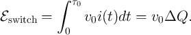
In order to compare the switching dynamic behavior (including the switching time and the switching
energy) predicted by the linear ionic model with some recently obtained experimental data,
let’s define  as the amount of charge that by passing through the memristor modulates the
memristance from its minimum to its maximum value (
as the amount of charge that by passing through the memristor modulates the
memristance from its minimum to its maximum value (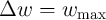 ). A voltage pulse with a fixed
amplitude of
). A voltage pulse with a fixed
amplitude of  and the duration of
  is applied to the memristor to perform an on-to-off (OFF)
switching.
is applied to the memristor to perform an on-to-off (OFF)
switching.
 | (3.9) |
where according to Eq. 3.8 we have
 | (3.10) |
Therefore,  is obtained as
 | (3.11) |
According to Eq. 3.11, derived from the linear ionic drift model,  has a constant value and is
independent of the
has a constant value and is
independent of the  and
and  . Therefore, it predicts that the switching time is inversely proportional to the
voltage pulse amplitude (
. Therefore, it predicts that the switching time is inversely proportional to the
voltage pulse amplitude ( ). Indeed, according to the State-dependent Ohm’s law for a memristive
system (Eq. 2.14), at a time
). Indeed, according to the State-dependent Ohm’s law for a memristive
system (Eq. 2.14), at a time  (
( ) where the electrical resistance of the memristor is
  (
( ), the rate of the charge flow (
 ) is directly proportional to the voltage pulse amplitude
(
) is directly proportional to the voltage pulse amplitude
( ). As a result, the amount of charge flowing through the memristor is proportional to the product of
the voltage level and the time (
). As a result, the amount of charge flowing through the memristor is proportional to the product of
the voltage level and the time ( ) and thus we have
  . As according to
the memristor linear ionic drift model
. As according to
the memristor linear ionic drift model  is a constant, the switching time required for a
complete switching from
is a constant, the switching time required for a
complete switching from  to
to  must be inversely proportional to the pulse amplitude
(
must be inversely proportional to the pulse amplitude
( ).
).
The OFF-switching energy consumption is also obtained as function of  by
by
 | (3.12) |
This predicts an inverse relationship between the switching energy and the switching time as 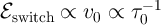 .
However, these predictions regarding the switching dynamic behavior (
.
However, these predictions regarding the switching dynamic behavior ( and
and 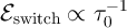 ) are
quite inconsistent with experimental data which demonstrate an inverse log-linear relationship between the
switching time and the voltage pulse amplitude as
) are
quite inconsistent with experimental data which demonstrate an inverse log-linear relationship between the
switching time and the voltage pulse amplitude as  [149] and a direct log-log
relationship between the switching energy and the switching time as
[149] and a direct log-log
relationship between the switching energy and the switching time as  [75].
The main reason is that the switching dynamic behavior is significantly affected by the electron
tunneling effect through the insulating region which exponentially decrease the total electrical
resistance of the TiO
[75].
The main reason is that the switching dynamic behavior is significantly affected by the electron
tunneling effect through the insulating region which exponentially decrease the total electrical
resistance of the TiO memristor device during the switching [138]. Therefore, although the
linear ionic drift model has been used to simulate the electrical properties of the memristor for
different applications [129, 130, 131, 132, 133, 87, 134], in a high voltage regime, however, the
tunneling effect dominates the memristor
memristor device during the switching [138]. Therefore, although the
linear ionic drift model has been used to simulate the electrical properties of the memristor for
different applications [129, 130, 131, 132, 133, 87, 134], in a high voltage regime, however, the
tunneling effect dominates the memristor  characteristics. For the sake of (acceptable) fast
switching, the applied voltage levels in logic applications are so high that the memristive devices
act as digital switches with two resistance states of
characteristics. For the sake of (acceptable) fast
switching, the applied voltage levels in logic applications are so high that the memristive devices
act as digital switches with two resistance states of  and
and  . As a result, it is necessary
to use a more accurate model for digital (logic) applications. The switching dynamic behavior
obtained from the nonlinear ionic drift model [138] explained below, shows a good agreement with
experimental data. For example, this model predicts a direct log-log relationship between the switching
energy and the switching time (
. As a result, it is necessary
to use a more accurate model for digital (logic) applications. The switching dynamic behavior
obtained from the nonlinear ionic drift model [138] explained below, shows a good agreement with
experimental data. For example, this model predicts a direct log-log relationship between the switching
energy and the switching time ( ) for both micro-scale (
 ) and
nano-scale (
) and
nano-scale ( ) TiO
) TiO memristive devices (see Fig. S7 in Supplementary Information
of [138]).
memristive devices (see Fig. S7 in Supplementary Information
of [138]).
3.3.2 Nonlinear Ionic Drift Memristive Model
To the author’s best knowledge, the nonlinear ionic drift model presented in [138], which uses the Simmons
 expression for the insulating region as a rectangular barrier with image forces [159], is up to
now the most accurate model for the TiO
expression for the insulating region as a rectangular barrier with image forces [159], is up to
now the most accurate model for the TiO memristive devices. By using physically reasonable
parameters, it properly describes both the static electric conduction as well as the switching dynamic
behaviors and provides a good fit to the experimental data from micro-scale and nano-scale
TiO
memristive devices. By using physically reasonable
parameters, it properly describes both the static electric conduction as well as the switching dynamic
behaviors and provides a good fit to the experimental data from micro-scale and nano-scale
TiO memristive devices which exhibit switching behaviors effectively insensitive to the device
size [138].
memristive devices which exhibit switching behaviors effectively insensitive to the device
size [138].
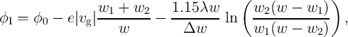
According to this model, the voltage across the thin-film is given by
 | (3.13) |
where  is the voltage across the insulating region which acts as a tunneling barrier and
  is the current
flowing through the device and its functional form is determined by [138]
is the current
flowing through the device and its functional form is determined by [138]
![[ ( √ -------)]
j0A (- B √ϕI) - B ϕI+e|vg|
i = ----2- ϕI e - (ϕI + e|vg |) e .
Δw](diss341x.png) | (3.14) |
The quantities from Eq. 3.14 are given by [138]
 | (3.15) |
 | (3.16) |
 | (3.17) |
 | (3.18) |
 | (3.19) |
where  describes the insulating region area,
  is the electron charge,
  is Planck’s constant,
  is the
barrier height,
is the
barrier height,  is the dielectric constant, and
  is the electron mass. The modulation of the effective
insulating region width
is the electron mass. The modulation of the effective
insulating region width  with respect to the device current has been expressed
for  (OFF switching):
![( ) [ ( ) ]
dw i w - ao ff |i| w
----= fo ff sinh ---- exp - exp ----------- --- - ---
dt ioff wc b wc](diss355x.png) | (3.20) |
with the fitting parameters 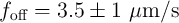 ,
,  ,
,  ,
,
 , and
, and  ;
;
and
for  (ON switching):
![( ) [ ( ) ]
dw i w - aon |i| w
---- = fon sinh ---- exp - exp --------- - --- - ---
dt ion wc b wc](diss362x.png) | (3.21) |
with the fitting parameters  ,
,  ,
,  ,
,
 , and
, and  for physical TiO
 memristive devices characterized in [138]. The
model fits the experimental data using the device parameters determined as
memristive devices characterized in [138]. The
model fits the experimental data using the device parameters determined as  ,
,
 ,
,  ,
,  [138].
The total resistance of the device (memristance) is equal to
 | (3.22) |
where  is the applied voltage on the memristor,
  is the current flowing through the device, and
 accounts for the Pt electrodes resistance [139].
This model properly describes the nonlinear switching dynamics arising from the ionic motion which
modulates the effective width of the insulating region (Eq. 3.20 and Eq. 3.21) as well as the electron
tunneling effect through the insulating region which is a function of the width of the insulating region and the
applied voltage/current (Eq. 3.14). Eq. 3.20 and Eq. 3.21 successfully model the nonlinear drift velocity of
ionized dopants [138] featuring an exponential dependence on the applied current/voltage [148] and the
asymmetric switching behavior [138] caused by the voltage polarity dependent competitive or cooperative
behavior of ionic drift and diffusion [147].
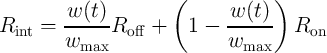
Fig. 3.4a shows the initial memristances (before any modulation in  ) for different values of
  as a
function of the applied voltage. It illustrates that the instantaneous value of the memristance
exponentially decreases with respect to the applied voltage during the switching. In fact, the electrical
resistance of the device depends on the applied voltage. Therefore, low-voltage measurements are
used to readout the memristance [75], which not only allows us to provide non-destructive reads
but also reduces the tunneling effect. Due to the coupling between Eq. 3.14 and Eq. 3.22, the
memristance needs to be calculated numerically. Fig. 3.4b shows the memristance as a function of
as a
function of the applied voltage. It illustrates that the instantaneous value of the memristance
exponentially decreases with respect to the applied voltage during the switching. In fact, the electrical
resistance of the device depends on the applied voltage. Therefore, low-voltage measurements are
used to readout the memristance [75], which not only allows us to provide non-destructive reads
but also reduces the tunneling effect. Due to the coupling between Eq. 3.14 and Eq. 3.22, the
memristance needs to be calculated numerically. Fig. 3.4b shows the memristance as a function of  when a readout voltage of 0.2 V is applied to the device. It illustrates that a sub-nanometer
modulation in the insulating region effective width provides a
when a readout voltage of 0.2 V is applied to the device. It illustrates that a sub-nanometer
modulation in the insulating region effective width provides a  readout ON-OFF-switching
regime [138].
readout ON-OFF-switching
regime [138].
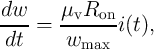
Fig.3.5 shows the dependence of the memristance during ON (high-to-low resistance) switching as it follows
from the linear and nonlinear ionic drift models. Due to a high voltage level applied ( ), the
tunneling effect trough the insulating undoped region dominates the memristor
), the
tunneling effect trough the insulating undoped region dominates the memristor  characteristics [138].
Therefore, during the switching, the total resistance is even lower than
characteristics [138].
Therefore, during the switching, the total resistance is even lower than  , in contrast to the behavior
predicted by the linear model according to Eq. 3.7. From Fig.3.5 one can see that the TiO
, in contrast to the behavior
predicted by the linear model according to Eq. 3.7. From Fig.3.5 one can see that the TiO component
announced by Hewlett Packard (HP) in 2008 [69], at least at high voltage regimes, is rather a memristive
system [70] than a memristor as its electrical resistance at a time is not only a function of historic profile of
the applied voltage/current but also of the instantaneous value of the applied voltage/current due to electron
tunneling. Furthermore, Fig. 3.5 demonstrates that when the linear model to obtain the
component
announced by Hewlett Packard (HP) in 2008 [69], at least at high voltage regimes, is rather a memristive
system [70] than a memristor as its electrical resistance at a time is not only a function of historic profile of
the applied voltage/current but also of the instantaneous value of the applied voltage/current due to electron
tunneling. Furthermore, Fig. 3.5 demonstrates that when the linear model to obtain the  characteristics of
  and
and  , the voltage drops
  and
and  (Eq. 3.4) will be wrongly predicted and
the implication gate optimization will not be reliable. The linear model can be useful only in
analysis and design of low voltage applications (
(Eq. 3.4) will be wrongly predicted and
the implication gate optimization will not be reliable. The linear model can be useful only in
analysis and design of low voltage applications ( ) where the tunneling is
negligible.
) where the tunneling is
negligible.
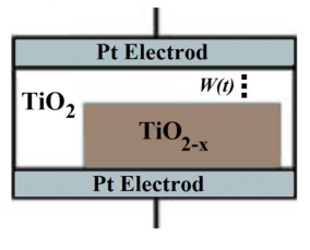
 memristive device cross section.
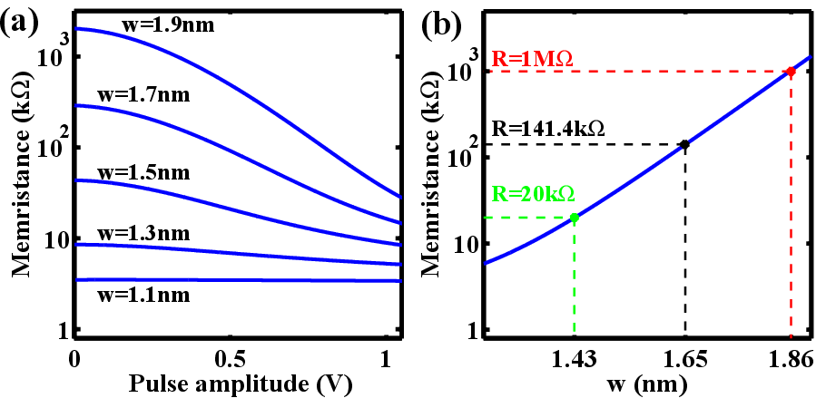
 characteristics of the TiO
 memristor for different values of
  . (b)
. (b)  characteristics
plotted for a readout voltage of 0.2 V.
characteristics
plotted for a readout voltage of 0.2 V.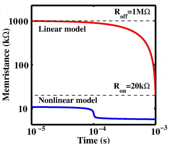
 memristive device during a high-to-low resistance switching according to
the linear and nonlinear models.
memristive device during a high-to-low resistance switching according to
the linear and nonlinear models.