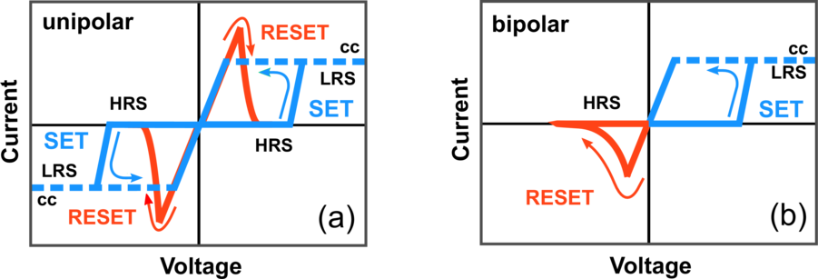
Figure 2.1: Schematic illustration of I - V curves during different type of resistive switching: (a) unipolar; (b)
bipolar [242].
First intensive studies of conductivity in metal-insulator-metal (MIM) structures were made in the 1960s and 1970s. At that time different phenomena, such as negative differential resistance [83], memory switching [82], threshold switching [177] were discovered and first extensive physical analysis of these effects was performed [47],[48],[49],[50], [76],[84],[216],[221]. The use of these phenomena for memory devices was proposed [55],[178]. But the early observations of resistive switching were not robust enough for real memory applications and these reports remained mostly in the domain of scientific studies [244].
Nowadays resistive switching memory is represented by RRAM, phase change RAM (PCRAM), and conductive bridge RAM (CBRAM) types.
CBRAM, also called in the literature as memory with an electrochemical metallization (ECM) [241] cell or a programmable metallization cell (PMC) [135], is based on an solid state electrolyte in which mobile metal ions can create a conductive bridge between the two electrodes under the influence of an electric field. The source of mobile metal ions is one of the electrodes, which is made from an electrochemically active metal, such as Ag, Cu, or Ni. Electrochemically inert metals, such as Pt, Ir, W, or Au are used for the second electrode [242].
PCRAM employs the difference in resistivity between crystalline and amorphous phases of a chalcogenide compound [143]. After the fabrication of devices a chalcogenide compound is in a crystalline phase. For a transition to an amorphous phase, a chalcogenide compound should be melted and rapidly quenched, for which a large electric current pulse is applied. For a transition back from the amorphous to the crystalline phase, a chalcogenide compound (operation region) must be annealed at a temperature between the crystallization temperature and the melting temperature, which is done by applying a medium electrical current pulse with time period sufficient for crystallization [245].
RRAM, also called in the literature as valence change memory (VCM) [242], exploits the phenomenon of the resistive switching in oxides.
Resistive switching is toggling the electrical conductance of the insulator in a MIM structure from the high resistance state (HRS) to the low resistance state (LRS) and vice versa by applying the electric field. The HRS can mean logical 1 and the LRS can mean logical 0, or vice versa, depending on the technology.
In 2000 Beck et al. and in 2001 Watanabe et al. reported an electrical resistive switching in Cr-doped SrZrO3 [14] and Cr-doped SrTiO3 [243], respectively. In 2004, Baek et al. [6] have demonstrated NiO memory cells integrated with the conventional complementary metal-oxide-semiconductor (CMOS) transistor in a one-transistor-one-resistor (1T1R) device structure. After that, the new phase of studying the resistive switching phenomenon and RRAM began. Resistive switching was shown in different materials/structures (Table 2.1).
| material | ref. | material | ref. |
|
| |||
| metal oxide
| |||
| NiO | [42],[132],[205], | CuxO | [59] |
| | [206],[207] | CoO | [208] |
| Nb2O5 | [213],[214] | ZnO | [34],[149],[250] |
| TiOx | [41],[63],[107], | HfO2 | [37],[38],[78], |
| | [109],[138],[139], | | [131],[146] |
| | [190],[209],[254] | SnO2 | [172] |
| ZrO2 | [144],[156] | Ga2O3 | [29] |
| MgOx | [110] | WOx | [22],[85] |
| Al2O3 | [155] | | |
| heterostructure of metal oxides
| |||
| AlOx/TiOx | [122],[127] | | |
| perovskite oxides
| |||
| Pr1-xCaxMnO3 | [202] | V-doped SrZrO3 | [154] |
| Nb-doped SrTiO3 | [215] | Fe-doped SrTiO3 | [170] |
The concepts of RRAM proposed in 2010 by Ho et al. (NDL) [85] and Kim et al. (Samsung) [127] have already surpassed the scaling limit of charge-based storage memories [39]. In 2013, RRAM has been demonstrated on a 32Gb test chip [160]. Despite the obvious progress in the last years, details about the physics of the switching mechanism remain an area of active research.
The switching event from LRS to HRS is called the RESET process and, conversely, the switching event from HRS to LRS is called the SET process. Usually, for fresh samples in its initial resistance state, a voltage larger than the SET voltage is needed to trigger the transition from HRS to LRS than during the subsequent cycles. This event is called the FORMING process. The FORMING/SET process is completed when the current in the system becomes equal to the compliance current (cc) level.
Depending on the relative polarities of the SET and RESET voltage, the resistive switching phenomenon is called either unipolar or bipolar (Figure 2.1). The switching operation is called bipolar, when the SET to LRS occurs at one voltage polarity and the RESET to the HRS at the opposite voltage polarity. The switching operation is called unipolar, when the switching procedure does not depend on the polarity of the write voltage [242].
| unipolar | bipolar |
| Pt/NiO/Pt [207] | Pt/NiO/SrRuO3 [42] |
| Pt/TiO2/TiN [254] | Pt/TiO2/TiN [68],[254] |
| Pt/TiO2/Pt [107],[190] | Pt/TiO2/Pt [107] |
| Pt/ZrO2/Pt [156] | Ti/ZrO2/Pt [156] |
| Al/ZrO2/Pt [156] | |
| TiN/HfO2/Pt [78] | TiN/HfO2/Pt [78] |
| Pt/HfO2/Pt [131] | |
| Ni/HfO2/TiN [38] | |
| Pt/ZnO/Pt [34] | TiN/ZnO/Pt [250] |
The switching behavior is not only dependent on the insulator material (Table 2.2) but also depends on the choice of the metal electrodes and their interfacial properties [125],[244]: Both switching types could coexist in one system. For example, Pt/TiO2/Pt shows both types of switching and the factor determining the switching type is the level of the cc (low cc (<0.1mA) activates bipolar switching; rather high cc (>1mA) activates unipolar switching).
Non-uniformity of device characteristics appears a major challenge for to large-scale manufacturing of RRAM. Significant parameter fluctuations exist in term of variations of the switching voltage as well as the resistances in HRS and LRS (RLRS/RHRS distribution). The variation of the resistive switching includes temporal fluctuations (cycle to cycle) and spatial fluctuation (device to device) [244]. The LRS resistance variation comes from the variation of the number or the size of conductive filaments, thus the reduction of possible filament paths effectively confines the active switching area and thereby may reduce the LRS variation. The HRS resistance variation comes from the variation of the ruptured conductive filaments length, thus any variation of the tunneling gap distance results in an exponential dependence of the tunneling current on the tunneling distance. Resistance variation could lead to a SET failure and re-RESET during SET process [8].
One of the potential methods to stabilize the characteristics of the resistive switching is the oxide doping. In 2012, Syu et al. [225] proposed the Si interfusion method to enhance the resistive switching characteristic of the WOx. Before Si enrichment the diverse oxidation states in the WOx film were providing the stochastic conduction paths, which lead to the irregular resistance switching behavior. The Si interfusion in WOx resistance switching layer can effectively localize the filament conduction paths to improve the resistance switching property.
To solve the problem of RRAM variability, first and foremost, one needs a better understanding and control of the SET/RESET processes. Development of accurate and flexible models of switching is paramount for future progress in RRAM technology [104].
Most switching materials show filamentary-type switching behavior. Filamentary-type switching involves the formation of a conductive path through an insulator layer, which leads to a transition to a LRS. The disruption of this path leads to a transition to a HRS. Non-filamentary-type switching has also been observed in several systems [22],[170],[215]. This type is also known as an interface-type switching [201]: it does not involve electroforming, and both SET and RESET switching appear as a rather gradual than abrupt process. Another distinct feature of the non-filamentary switching is that the system resistance depends on the cell size [108].
In the literature several physical mechanisms/models have already been suggested for the explanation of SET/RESET processes (Table 2.3).
| macroscopic level | microscopic level |
| [28],[32],[33],[67],[124], | [72],[73],[174],[192],[249] |
| [126],[128],[151],[173],[194], | |
| [195],[196],[200],[226] | |
The first suggestion about filamentary conduction and switching for unipolar behavior was made by Dearnaley [47] in 1967. Dearnaley did not specify conductive filaments at the atomic level, although he suggested some possible models such as Si-O-Si chains in SiOx [47] and, more generally, Mz+-Mz+ chains [48]. In this model, the RESET switching is a result of the rupture of the conductive filaments in the insulating matrix by Joule heat, while a mechanism for SET switching is assumed to be a recovery of the ruptured conductive filaments. The mechanism based on these processes is called the fuse-antifuse type [242] and is most commonly used to describe unipolar switching. Dearnaley’s ideas were future developed in the macroscopic SET and/or RESET models proposed by Sato et al. [200], Russo et al. [194],[195],[196], Cagli et al. [28], Lee et al. [151], Ielmini et al. [99], and Bocquet et al. [25] for describing the resistive switching behavior in NiO and/or TiO2. In these publications the RESET switching is explained by dissolution of conductive filaments owing to Joule heat. According to the results of simulations the conductive filament rupture/recombination should occur in the middle of the filament. However, several experimental works have shown that the switching-determining region is rather located at the interface between anode/NiO [132], anode/TiO2 [123], and cathode/NiO [121]. Thus the conductive filament breaking should occur in this region. Kim et al. [124],[126] have solved the problem by assuming a cone-shaped conductive filament for TiO2, NiO. This form of the conductive filament involves heating in a tight spot and a formation of the hottest place at the interface, where, according to the experimental results [121],[123],[132], the rupture occurs. The existence of more than one filament in a single memory cell was suggested [1],[120],[145],[150], and several aspects of such a switching in NiO were modeled by Kinoshita et al. [133].
Attempts to explain resistive switching phenomenon at the atomistic level were undertaken by Chudnovskii et al., in 1996 [43]. Their predictions were based on a simple free energy calculation of a lower oxide (with lower stoichiometric oxygen concentration) formation reaction. They presupposed that the resistive switching behavior is due to the phase transition from a highest oxide (HRS) to a lower oxide (LRS), e.g. TiO2 ⇄TinO2n-1 (n = 4..9). This reaction is spontaneous and could be accelerated by Joule heating during FORMING/SET processes. Note that this calculation is only valid for a transition metal oxide (TMO) film on an metal electrode. In 2010, Kwon et al. [139] directly observed the nanoscale conductive filaments in a Pt/TiOx/Pt memory cell by high-resolution transmission electron microscopy (HR-TEM), and identified the cone-shaped conductive filaments composed of the oxygen-deficient Magn´eli phase, e.g. Ti4O7.
A non-thermal approach to a unipolar switching was proposed by Chae et al. [32]. In this model the SET/RESET switching is based on a random circuit breaker network. Simulation results can mimic the experimental behavior, but the model lacks the detailed physics of the circuit breakers [108].
The first attempts to explain the bipolar switching were made by the pioneers in the field in the 1960s and 1970s. In 2000, Beck et al. [14] suggested that charge-transfer processes via donor and acceptor levels (Cr3+ and Cr4+) appear to be the mechanism for carrier creation and transport within the Cr-doped insulator SrZrO3. Then in 2001, Rossel et al. [191] concluded that the current flows through localized channels/filaments rather than homogeneously across the bulk of the film. This current is mainly due to the hopping or tunneling of charges between the adjacent sites or traps localized in the gap of the insulator. The conductive filament formation and rupture should be coupled with structural change. Tsui et al. [231] proposed a conduction mechanism via crystalline defects generated by the applied electric field. Later, the change in the conductivity of conductive filaments in Cr-doped SrZrO3 was explained as the oxygen vacancy drift along the applied electric field [106]. Then, Jeong et al. [109] proposed a mechanism for bipolar switching in TiO2 based on oxygen vacancies (V o) migration.
A non-filamentary approach to bipolar switching was suggested by Sawa et al. [202] in 2004. They concluded that the resistive switching in Ti/Pr0.7Ca0.3MnO3/SrRuO3 can be explained by an interface model of Ti/Pr0.7Ca0.3MnO3 which has a sufficiently [145] high density of traps to form a Schottky-like barrier. This mechanism of resistive switching was adopted by Fujii et al. [67] to interpret the switching in Au/SrRuO3/SrTi0.99Nb0.01O3.
A phenomenological model which may explain several particular aspects of the bipolar switching phenomenon was proposed by Rozenberg et al. [192],[193]. The insulating medium contains metallic domains, which in explicitly correspond to charge traps in the real system such as dopants, vacancies, metallic clusters, and nanodomains. It is assumed in this model that there are just three types of domains. The top and bottom domains are taken to be smaller than the middle one. This domain differentiation might be justified by the different properties of the electronic states close to the interfaces of the metal electrodes. Electric current is carried by electrons hopping between the domains as well as between a domain and an electrode, when an external voltage is applied. Resistive switching is explained on the basis of filling and desolating these domains.
One of the first microscopic SET/RESET mechanism for bipolar switching was proposed by Xu et al. [249], and termed the “unified physical model”. It is based on the following assumptions:
In [73], Gao et al. presented an extension of “unified physical model” as follows: O2- are mainly accumulated at the interface between the electrode and the resistive layer and can jump over the interface barrier under an applied electric field. In [72] authors investigated the system in its LRS and showed, that the switching-determining region is formed near the cathode in the case of bipolar switching and near the anode in the case of unipolar switching.
At this stage of the investigation of resistive switching first explanations of phenomena were proposed. First macroscopic and phenomenological models, that could explain one or another experimental observation, were developed. The first experimental observation of a conductive filament was provided. Despite the fact that some ingredients of microscopic mechanisms have also been suggested the microscopic model capable of reproducing a resistive switching behavior in oxides (FORMING/SET and RESET process) was not provided.
Lately the number of papers devoted modeling the resistive switching phenomena has rapidly increased (Table 2.4).
| macroscopic level | microscopic level |
| [21],[25],[96],[97],[99], | [18],[19],[20],[38],[51], |
| [133],[147],[152],[161],[251] | [52],[70],[71],[74],[91], |
| | [92],[98],[142],[162],[193], |
| | [197],[232],[233],[234],[256], |
| | [257],[258],[259],[266] |
By extending the main assumptions of the “unified physical model” a microscopic stochastic model of the resistive switching was developed (Chapter 3). The improvement of the “unified physical model” is continuously ongoing:
In [257, 256] the TAT was added to the “unified physical model”.
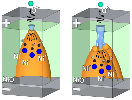
In 2010, Yoo et al. [252] and Hwang et al. [95] observed a dendrite-like conductive filament in NiO layer (Figure 2.2). In this case the resistive switching occurs as follows [125]:
Phenomenological models which explain several particular aspects of the bipolar switching phenomenon were also proposed by Bertin et al. [21], Liu et al. [161], Yu et al. [259], Sasaki [197], etc. Non-filamentary models for unipolar switching were also reported in the literature, e.g. Xue et al. have suggested a model based on the Mott-Hubbard metal-insulator transition picture [251].
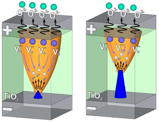
A fully microscopic study of SET/RESET process in the case of unipolar switching in Pt/TiOx/Pt (Figure 2.3) was presented in [266]. The authors concluded that:
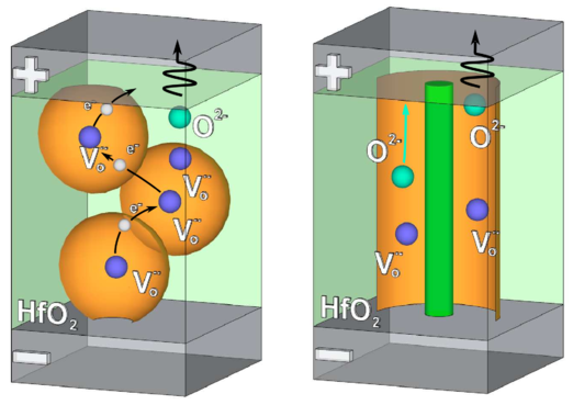
Bersuker et al. [18] proposed a microscopic filamentary-type model of resistive switching for TiN/HfO2/TiN (Figure 2.4). They claimed that:
Thus the population of electrically active V o+ traps decreases closer to the anode. Several aspects of this model were also discussed in the earlier work by the same group [19],[20],[232],[233],[234]. In a macroscopic approximation model based on a practically similar mechanism for HfO2 was done by Ielmini [96],[97]. Lerantis et al. [142] and Ielmini et al. [98] have presented an alternative numerical RESET microscopic model for HfO2. In 2013, Kalantarian et al. [113] showed the mechanism of the RESET process in HfO2, where the RESET process occurs due to the migration of O2- ions stored in the bulk of the oxide layer.
Degraeve et al. [51],[52] have suggested a conductive filament in an “hour glass” form for TiN/HfO2/Hf/TiN. In this model the conductive filament never breaks but only narrows. A potential barrier is raised in the constriction due to quantum mechanical confinement, which blocks the current. Another distinctive feature of this model is the absence of Vo generation/recombination and the whole resistive switching process is due to the Vo flow from one part of the “hour glass” to another, and vice versa. In [182], an extension of the “hour glass” model was presented, which considers the event of conductive filament breaking.
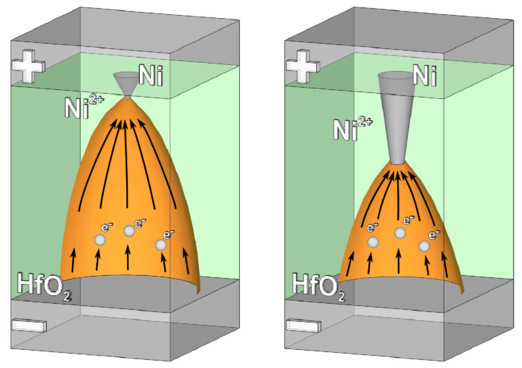
In 2012, Chen et al. [38] have observed unipolar resistive switching in Ni/HfO2/TiN and proposed the resistive switching mechanism (Figure 2.5) as follows:
Recent experiments have shown that use of a stacked oxide RRAM structure is one of the most promising methods to improve the properties of this type of memory [40],[79],[87],[129],[152],[246]. In [79] the authors used a quantum-point contact model [53] for modeling of filament-resistance states.
In Oct. 2013, Kamiya et al. [115],[116] has proposed a possible mechanism, the vacancy “Cohesion-Isolation” phase transition, for explanation of resistive switching in stacked oxides Al2O3/HfO2/Hf [79] in microscopic level. Several aspects of this mechanism were also discussed in the earlier work of this group [114],[211].
Resistive memory has come a long way from the early works to prototyping of the RRAM arrays. Currently, oxide-based resistive memory is widely accepted as a potential candidate of the future universal memory. One of the main advantages of a RRAM is its simple structure. The RRAM prototypes have already surpassed the scaling limits of charge-based storage memories. However, the main challenge of this type of memory is the non-uniformity of device characteristics. To solve these problems one needs a better understanding and control of the SET/RESET processes. Development of accurate and flexible models of switching is paramount for future progress in RRAM technology.
In early works macroscopic and phenomenological models, which could explain one or another experimental observation were proposed. The first experimental observation of a conductive filament was provided. Despite the fact that some microscopic mechanisms have been suggested, a microscopic model capable of reproducing the resistive switching behavior in oxides (FORMING/SET and RESET process) was not provided.
Work on the description and clarification of the resistive switching phenomenon continues today. The mechanisms for filamentary-type switching phenomena are not completely understood, although up to now experimental evidence supporting one or another hypotheses have been revealed. The current state-of-the-art understanding of the problem lies in the fact that the resistive switching is associated with the structural changes within the oxide, i.e. the formation/annihilation/migration of the defects, and an electron transport through these defects.
The first full stochastic model of the oxide resistive switching, based on some variation of the “unified physical” mechanism was developed. The main advantage of this stochastic model is that for the first time movement of oxygen ions and electron hopping were taken at equal footing, which allowed us to describe the full cycle of resistive switching, as will be shown in Chapter 3.