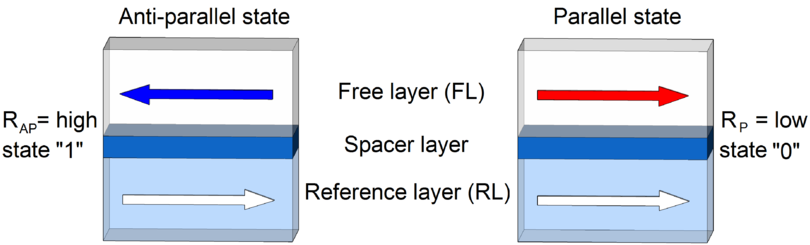
Figure 4.1: Schematic illustration of a magnetic pillar in a high resistance (left) and low resistance (right) state.
First suggestions for memory which uses magnetism for storage information were given in the 1950s. One of the first a so called magnetic core memory was proposed, where small magnetic toroids (ring of ferrite material) were used. Through these rings the wires for read and write information were threaded. Toroids can be magnetized either clockwise or anti-clockwise regarding the axis of rotation going through it. These two magnetization states are mapped to 0 and 1. This type of memory has been used as one of the first non-volatile methods for information storage. Magnetic core memory was widely used for almost 20 years until the advent of the semiconductor memory [204].
In 1969, Bobeck et al. [24] proposed a magnetic bubble memory, where information is stored in cylindrical domains or bubbles, each bubble storing one bit. The bubbles were created by a generator signal in a thin magnetic film, were pushed through the film in a racetrack by the external a magnetic field and detected by a sensor [222].
Nowadays, magnetic memory technology is represented by magnetoresistive RAM (MRAM) and spin transfer torque MRAM (STT-MRAM).
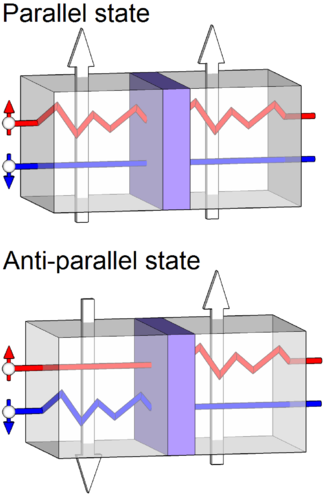
The basic element of a MRAM and STT-MRAM is a sandwich of two magnetic layers separated by a non-magnetic conducting spacer layer or a thin insulating layer. While the magnetization of the reference layer (RL) is fixed due to the fabrication process, the magnetization direction of the free layer (FL) can be switched between the two states parallel and anti-parallel to the fixed magnetization direction. Anti-parallel and parallel states possess different magnetoresistances which are mapped to 0 and 1 (Figure 4.1).
The two most important magnetoresistance phenomena consists of the giant magnetoresistance (GMR) and the tunnel magnetoresistance (TMR) effect.
In the late 1980s, Baibich et al. [7] and Binasch et al. [23] have independently observed GMR in Fe/Cr superlattices. GMR is detected in a pillar consisting from at least two ferromagnetic layers separated by a non-magnetic conducting spacer layer. The resistance of the pillar depends on the layers magnetization direction relative to each other.
To quantify the GMR effect the following ratio was introduced [262]:
 | (4.1) |
Here, RAP and RP are the resistances, ρAP and ρP are the resistivities, σAP and σP are conductivities in the high (anti-parallel) and low (parallel) resistance state, respectively. According to Equation 4.1 the GMR can be much larger than 1, if ρAP > ρP . An alternative definition the GMR less than 1 (ρAP > ρP ) describes as [262]:
 | (4.2) |
In a first approximation one can assume that two independent channels of conductivity exist for electrons with “spin-up” and “spin-down” orientations [181]. The total current is the sum of the I↑ current carriers with “spin-up” and the I↓ current carriers with “spin-down”. If the currents I↑ and I↓ are flowing through the ferromagnetic layer with a fixed direction of magnetization (“up” or “down”), the resistance of the first and second groups of electrons differs.
The source of the GMR (Figure 4.2) is the unequal scattering of the two groups of electrons with different spin orientations with respect to the magnetization direction of the ferromagnetic layer [181]. If the magnetization direction of the ferromagnetic layers are the same (parallel state), the “spin-down” electrons (spin is anti-parallel to the magnetization) can propagate through the structure nearly unscattered, resulting - thereby in high electron conductivity and hence a low resistance. In contrast, in the anti-parallel state both “spin-up” and “spin-down” electrons undergo collisions in ferromagnetic layers, leading to a high resistance [35].
This technology was adopted for hard disk drive read heads and stimulated the new phase of research in magnetic memory, as GMR-based MRAM [227].
In 1975, Julliere et al. discovered the phenomena of the tunnel magnetoresistance (TMR) in a Fe/Ge/Co junction at T ≤4.2K [111]. TMR is detected in a pillar consisting from two ferromagnetic layers separated by a thin insulating layer (magnetic tunnel junction (MTJ)). The resistance of the pillar, as in the GMR case, depends on the magnetization direction layers with respect to each other.
To quantify the TMR effect the following ratio is commonly used [102],[119]:
 | (4.3) |
Here, RAP and RP are resistances in the high resistance state and the low resistance state, respectively.
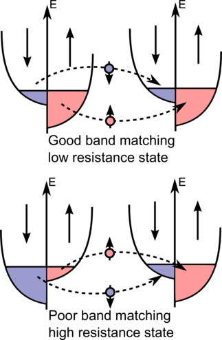
The simplest interpretation of the TMR effect can be done as shown in Figure 4.3. The electrons with certain spin orientation (“spin-up” or “spin-down”) can tunnel from one ferromagnetic layer to another ferromagnetic layer through a non-conductive thin insulating layer if there are available free states with the same spin orientation. In case of the parallel state, the majority spin (“spin-up”) electrons and minority spin (“spin-down”) electrons can easily tunnel to the second ferromagnetic layer and fill majority (“up”) and minority (“down”) states, respectively. This will result in the large conductance and corresponds to the low resistive state. In case of the anti-parallel state, the majority spin (“spin-down”) electrons and minority spin (“spin-up”) electrons from first ferromagnetic layer fill the minority (“down”) and majority (“up”) states in the second ferromagnetic layer, respectively. This will result in the low conductance and corresponds to the high resistive state.
Despite the fact that the TMR effect was demonstrated earlier than GMR, its use in memory became possible only after observing large TMR in structures with amorphous Al2O3 tunnel barriers. First independent developments of structures with amorphous Al2O3 tunnel barriers were performed by Moodera et al. [169] and Miyazaki et al. [166]. The largest TMR ratio of an MTJ with amorphous Al2O3 is equal to 70.4% at room temperature and was demonstrated by Wang et al. [240], in 2004.
The next breakthrough in the development of magnetic memory was the discovery of a giant TMR in an epitaxially grown MTJ with MgO barrier. In 2001 a giant TMR in an MTJ with MgO barrier was independently predicted by Butler et al. [27] and Mathon et al. [164]. Mathon et al. [164] predicted the TMR ratio for an MgO barrier in excess of 1000%. By nature, this effect occurs from the symmetry-based spin filter effect in the MgO barrier [119]. The first experimental observation of TMR in Fe/MgO/FeCo(001) single-crystal epitaxial junctions was made by Bowen et al. [26]. The experiments showed a much smaller value of TMR (27% at 300K, 60% at 30K). In 2004 Parkin et al. [179] and Yuasa et al. [261] demonstrated TMR in single-crystal Fe/MgO/Fe MTJs up to 220% and 180% at room temperature, respectively. The TMR of the epitaxial MTJ increased rapidly, thanks to the rapid progress in fabrication techniques [102]. In 2006, Yuasa et al. [260] have shown TMR up to 410%. In 2008, Ikeda et al. observed giant TMR effects up to 604% at room temperature and 1144% at 4.2K in junctions of Ta/Co20Fe60B20/MgO/Co20Fe60B20/Ta [100].
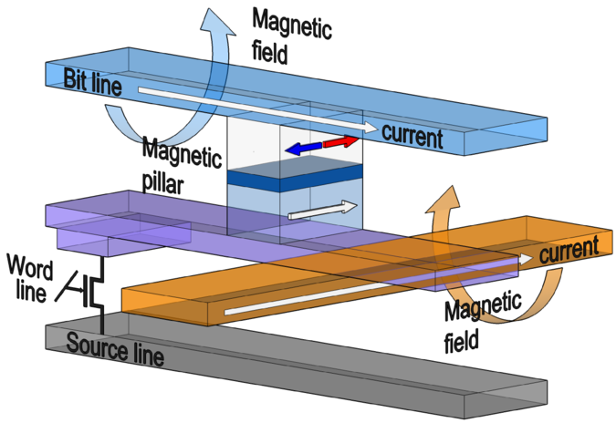
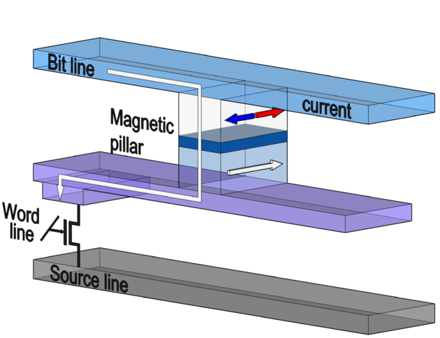
In conventional field-induced MRAM the free layer magnetization switching is performed by applying a magnetic field (Figure 4.4). The writing operation is carried out by the current flowing through the wires. The currents generate a magnetic fields around the wires. Switching occurs in the cell only, if the magnetic fields from both currents are present at the magnetic pillar. This protects cells disposed along one of the wires from spontaneous switching. The current required for generating the magnetic field for the switching increases when the wire cross-section decreases, leading to the problem of scaling MRAM cells. Therefore, MRAM cells based on a magnetic field switching exhibit a scalability limit of about 90nm [204].
In contrast to field-induced MRAM, STT-MRAM does not require an external magnetic field. Switching between the two states occurs due to the spin transfer torque produced by the spin-polarized current flowing through the pillar (Figure 4.5). The theoretical prediction of the spin transfer torque effect was made independently by Slonczewski [217] and Berger [16]. In general, when electrons pass through the thick fixed magnetic layer, the spins of the electrons become aligned with the magnetization of this layer. When these spin-polarized electrons enter the free layer, their spin orientations are getting aligned with the magnetization of the free layer within a transition layer of a few angstroms. Because of their spin orientation changed in the free layer, they exert a torque on the magnetization of the layer, which can cause magnetization switching, if the torque is large enough to overcome the damping. Smaller torque values result in magnetization precession around the effective magnetic field. By changing the current polarity the magnetization of the free layer can be switched from the anti-parallel to the parallel state and back with respect to the reference layer. In general, scalability is not a problem for the STT-MRAM cell, since reducing the size of the cell leads to a reduction in the current required for switching [204].
The interest in MRAM has increased significantly after the observation of spin-torque induced switching on all-metallic stacks [204], which happened long after the theoretical prediction of this phenomena. GMR-based Co/Cu/Co was the first pillar where spin-torque induced switching [80],[117],[171],[219],[230] was shown. First AlOx-based and MgO-based STT-MRAM cells were shown in 2004 [88] and 2005 [56], respectively.
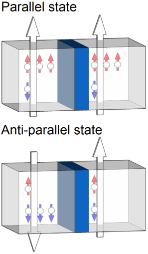
Depending on the orientation of the layer magnetizations the magnetic pillars can be divided into two categories (Figure 4.6): “perpendicular” with out-of-plane magnetization direction and “in-plane” with magnetization lying in the plane of the magnetic layer.
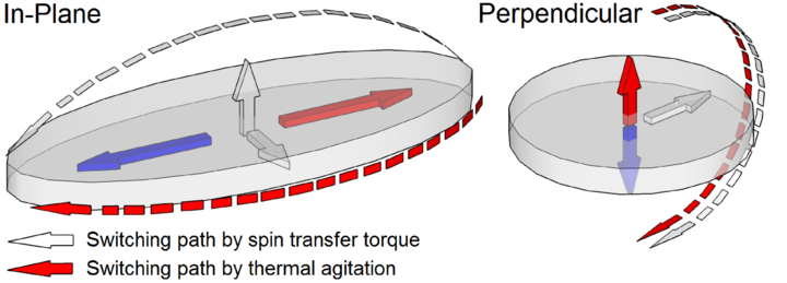
Switching of the magnetization can occur not only under the influence of the spin-polarized current, but also spontaneously due to thermal fluctuations (Figure 4.6). This is an unwanted event which leads to the loss of stored information. Thus, an important parameter of MRAM (STT-MRAM) is the thermal stability factor which is defined as the ratio of the thermal stability barrier to the operating temperature [101]:
 | (4.4) |
Here, Eb is the energy barrier that separates the two magnetization states, kB is the Boltzmann constant, T is the temperature. The energy barrier is defined as Eb = MSHKV/2 [101], where MS is the saturation magnetization, HK is effective anisotropy field, V is the volume of the free layer.
The thermal stability factor for perpendicular MTJs (p-MTJs) is given by the interface-induced perpendicular anisotropy field HKperp (H K = HKperp - 4πM S) as [3],[203]:
 | (4.5) |
To increase the thermal stability factor it is sufficient to increase the cross-section of p-MTJs, however, due to the domain formation, the cross-section is limited to approximately 70nm diameter, and, therefore, increasing the thermal stability factor of the single free layer p-MTJs above 40-50 is challenging [198],[199].
The thermal stability factor for in-plane MTJs is determined by the shape anisotropy field HKin-plane (H K = HKin-plane) [3],[203]:
 | (4.6) |
Therefore, to increase the thermal stability factor it is sufficient to increase the thickness of the free layer and/or the aspect ratio between principal axes defining the elliptical cross-section.
The (critical) switching current Ic is the current that is needed for switching the free layer from its actual magnetization direction to the opposite direction. However, it is not the switching current, but the switching current density counts, i.e. Jc = Ic/Acs, where Acs is the cross-section area of the free layer. The spin-polarized current is only a fraction of the total charge current flowing through the device. Therefore, high current densities from ~ 107 to ~ 108A/cm2 are required to switch the magnetization direction of the free layer, and the reduction of this required current density for switching is the most important engineering challenge for the STT-MRAM devices.
In p-MTJs the switching paths by spin transfer torque and thermal agitations (Figure 4.6, left) are the same. Thus, the critical switching current for p-MTJs is proportional to the thermal stability factor [3]:
 | (4.7) |
Here, η is the polarizing factor [217],[30], α is the Gilbert damping parameter, e is the electron charge, μ0 is the magnetic constant, ℏ is the reduced Planck constant.
In in-plane MTJs the switching under the influence of the spin current is following a different path than under the thermal agitations (Figure 4.6, right). Along this path the magnetization must get out of plane. This leads to an additional large term 2πMS2V in the switching current [3]:
 | (4.8) |
which results in a higher critical current compared to that in p-MTJs.
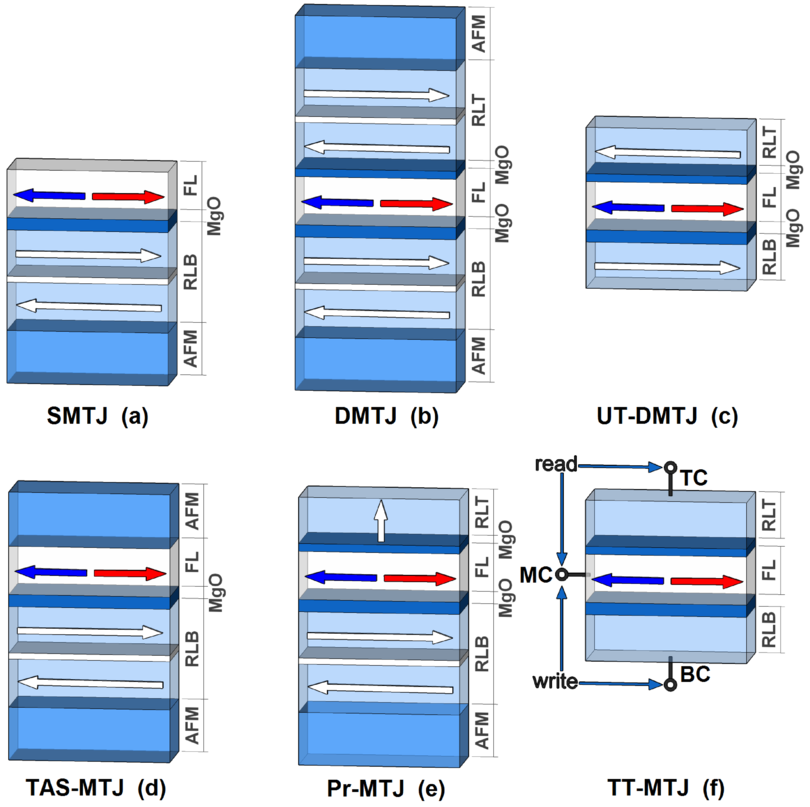
Typical pillar designs for STT-MRAM cells are illustrated in Figure 4.7. In all the structures (except the Pr-MTJ (Figure 4.7e)) instead of layers with in-plane magnetization layers with perpendicular magnetization can be used. The spacer layer is made from a non-magnetic conducting material (in the case of the GMR-based devices) as well as insulating oxides.
The single MTJ with one tunnel barrier (SMTJ) (Figure 4.7a) is the simplest structure. It consists of one reference layer, a spacer layer, and a free layer. The reference layer should be more stable than the free layer in order to prevent the spontaneous switching of the reference layer during memory operations. The reference layer is made as a synthetic antiferromagnet (SAF). An SAF comprises two magnetic sublayers with opposite magnetizations separated by a thin ruthenium layer to provide a strong exchange coupling between the sublayers. At the same time, the opposing magnetizations of the sublayers allows to minimize the impact of magnetostatic influence of the reference layer onto the free layer. The reference layer is usually strengthened with direct exchange-bias coupling to an antiferromagnetic layer (AFM). The free layer can be formed as SAF, which leads to an increased thermal stability.
The dual MTJ with two barriers (DMTJ) (Figure 4.7b) is the structure consisting of the reference layer/spacer layer/free layer/spacer layer/reference layer [58],[66],[89]. During the switching process the second reference layer provides an extra spin-torque. In the anti-parallel configuration of the reference layers (the magnetizations of the two reference layers are anti-parallel), the spin currents from either of the reference layers exert torques in the same direction (full torque is the sum of the individual torques), while in the parallel configurations, the torques are in the opposite directions (full torque is the difference of the individual torques) [64]. Thus switching current can be reduced by almost 2 times [58] in the anti-parallel configuration.
A disadvantage of this structure is the reduced magnetoresistance. Since reference layers are in anti-parallel configuration, one part of the structure (a reference layer and the free layer) is always in a low resistance state while another part is in a high resistance state. This disadvantage can be easily solved by the use of different thicknesses of spacer layers or different materials for each of the spacer layers.
In order to reduce the overall thickness of the cell in ultra-thin dual MTJ (UT-DMTJ) (Figure 4.7c) each reference layer is not built as a SAF but as a single ferromagnetic layer. The magnetostatic interaction between them further strengthens the anti-parallel configuration of the reference layers.
Thermally assisted switching (TAS) mechanism is used in several designs of the magnetic cell [180]. In the first design of TAS cell a free layer composed from a ferromagnetic material with low Curie point was used [15],[46]. The free layer is heated close to the Curie temperature and after that is switched to a desired direction by applying a small magnetic field. In the second design an interface coupling between the antiferromagnetic layer and the ferromagnetic layer is used as the storage mechanism [46]. Both layers are heated above the N´eel temperature and then cooled in the presence of a magnetic field in the write direction. The N´eel temperature of the antiferromagnetic material is lower than the Curie temperature of the ferromagnetic material. Thus, a relatively modest current is required to heat both layers above the N´eel temperature. In principle, both these designs are covered by the structure shown in Figure 4.7d.
The cell utilizing precessional switching mechanism (Pr-MTJ) (Figure 4.7e) is the structure in the form of the reference layer with the in-plane magnetization/spacer layer/free layer with the in-plane magnetization/spacer layer/reference layer with the perpendicular magnetization [118]. The reference layer with the in-plane magnetization is used for readout of the magnetic state of the free layer. The reference layer with the perpendicular magnetization is used for the switching operation. During the switching operation, the spin-torque from the reference layer with perpendicular magnetization affects the magnetization of the free layer causing the magnetization of the latter to tilt out of the plane. This leads to a large demagnetization field perpendicular to the plane of the free layer. This demagnetization field forces the magnetization of the free layer to precess about the direction normal to the free layer plane. Simulations of Pr-MTJ demonstrate that the switching time can be less than 50ps [118]. The switching time of 500ps [159] was demonstrated experimentally. Additional improvement of the design is still required to guarantee the necessary free layer final state [158].
All of the above designs are made on two-terminal devices with writing based on the spin-polarized current and reading based on magnetoresistance (TMR or GMR). These two operations have different requirements for the device. For writing high spin-currents are needed. The memory cell is required to have the resistance around or below the CMOS field-effect transistor (FET) impedance to guarantee sufficient write current. However, for reading the memory cell resistance must be well above that of the FET impedance to improve the read signal [220].
For the solution of this difficulty a three-terminal MTJ cell (TT-MTJ) was proposed (Figure 4.7f) in which different paths are used for read and write operations [220]. As shown schematically in the Figure 4.7f additional terminal (middle contact (MC)) is connected to the free layer along with the usual terminals (top contact (TC) and bottom contact (BC)). The read operation is performed by applying a voltage between the TC and MC. Write operation is carried out by applying a voltage between the BC and MC [119].
MTJ-based STT-MRAM is widely recognized as the most promising candidate for future universal memory. There are two competing classes of MTJs with different directions of magnetization of the free layer: in-plane and perpendicular. Each of the classes has advantages, and disadvantages. Perpendicular MTJs with an interface-induced anisotropy show potential, but still require a reduction of damping and an increase of thermal stability. The in-plane MTJs exhibit a high thermal stability, but still require a reduction of the critical current density. Micromagnetic simulations significantly contribute to solving this problem through the optimization of STT-MRAM memory cells. In Chapter 7 a new design of the in-plane structure is presented.