Chapter 8
Magnetization Oscillations in MTJ-based Structures
8.1 Switching Failure in a MTJ-based STT-MRAM
During the comparison between the switching time of the structure with composite and monolithic free layers, it has been
found that for a structure with the geometry CoFeB(5nm)/ MgO(1nm)/CoFeB(3.5nm)/MgO(1nm)/CoFeB(5nm) and a
monolithic free layer with an elliptical cross-section 52.5 × 15nm2, a large percentage of switching was finished with failure
(i.e. did not result to opposite magnetization state). In this section the switching probability of in-plane penta-layer MTJs
for different switching current densities and pulse durations is investigated.
First the dependence of the switching statistics on the current density and pulse duration (Figure 8.1, Figure 8.2) is
investigated. For that purpose 100 switching cycles under the current density 2.5 ⋅ 106A/cm2, 5 ⋅ 106A/cm2,
and 7.5 ⋅ 106A/cm2 and a pulse time of 30ns have been simulated. The state of the system at time intervals
of multiples of 0.5ns was taken, and for each of these states 10 relaxation processes under the influence of
temperature were computed. This gave 1000 simulation realizations of the switching process for each pulse
duration (multiple of 0.5ns) and for each of the three values of the current density for switching probability
evaluation.
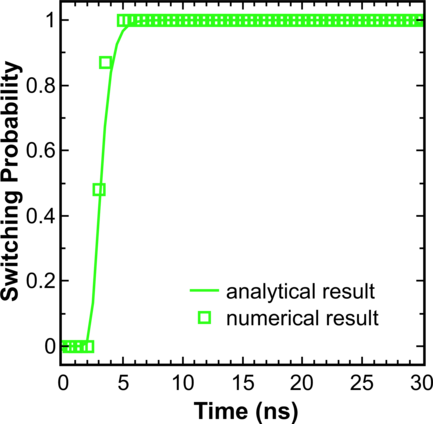
Figure 8.1 shows that for a current density 7.5 ⋅ 106A/cm2 the numerical solution is in good agreement with the
analytical expression:
 | (8.1) |
Here, tp is duration of the current pulse, Δ is the thermal stability factor. For φ the equation from [57] is
used:
 | (8.2) |
Here, η is the spin polarization factor, μB is the Bohr’s magneton, e is the electron charge, MS is the saturation
magnetizations, d is the thickness of the free layer, jc is the critical current density, j is the current density
(j > jc).
Next, it was found that the switching probability for the current density 5 ⋅ 106A/cm2 is equal to one when
the pulse is longer than 26.5ns. This pulse duration is longer than the respective value of 23ns needed to
achieve the ultimate switching at the current density 2.5 ⋅ 106A/cm2 (Figure 8.2). Interestingly, for the current
density 5 ⋅ 106A/cm2 and a pulse duration between 8ns and 26.5ns the switching probability is less than one
and fluctuates. This is in striking contrast to the earlier results, where the increasing pulse duration and
current density always leaded to the switching probability increase [31]. To determine the reason for this
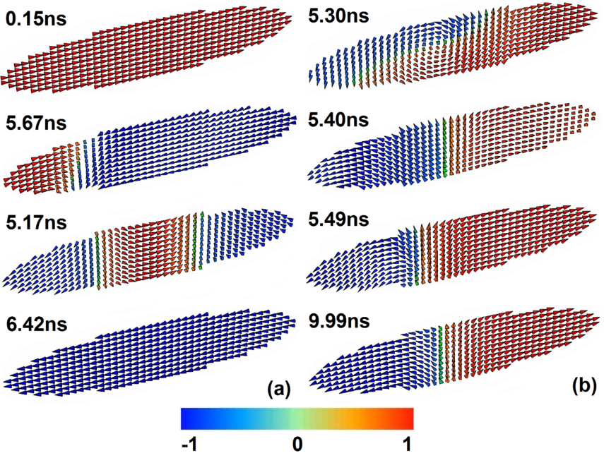
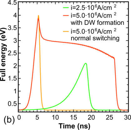
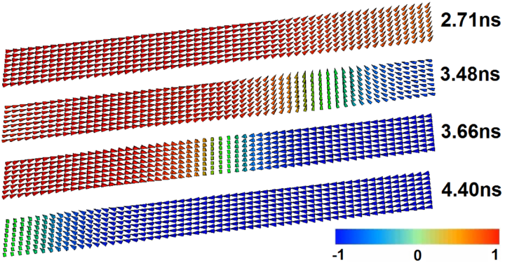
discrepancy, the switching process is investigated in detail (Figure 8.3). It was found that during some of the
switching realizations at the current density 5 ⋅ 106A/cm2 a vortex is created (Figure 8.3b, 5.3ns). The formation
of the vortex state in films thicker than 3.2nm is fully consistent with the results obtained previously for
three-layer structures with a synthetic free layer [253]. After the vortex is formed, it transforms into a transverse
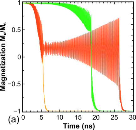
domain wall (Figure 8.3b, 5.4ns). After that the transverse wall starts oscillating around the center of the free
layer with an increasing amplitude (Figure 8.4a), which leads to the increase of the switching time. At a
lower current density the domain wall is not formed and the switching proceeds normally (Figure 8.3a). The
formation of the transverse domain wall is possible at higher currents, when the switching energy barrier for
normal switching is practically equal to the formation energy barrier of the vortex/transverse domain wall state
(Figure 8.4b).
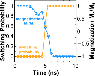
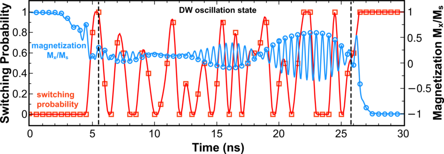
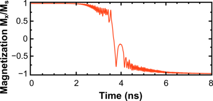
Next, the validity of the criterion typically used to describe the 100% switching is investigated. As illustrated in
Figure 8.5, in the case of normal switching from 1 to -1 the switching probability is defined to be 1 if the normalized average
magnetization Mx∕MS along the long axis becomes less than -0.5 (Mx∕MS < -0.5) [31]. If, however, the vortex
state is generated, due to the oscillatory behavior of the domain wall the 100% switching can be achieved
even when Mx∕MS > 0.5 (Figure 8.6). This exception demonstrates that in making a decision about reliable
switching one has to consider not only the average magnetization but also the state of the system during
switching.
8.2 MTJ-based Bias-Field-Free Spin-Torque Oscillator
Detected oscillations in the penta-layered structure are parasitic and undesirable phenomenon in structures used for
MTJ-based memory. However, this effect can be utilized for spin-torque oscillators. Spin-torque oscillators together with
STT-MRAM are the new types of spintronics devices utilizing all-electrical magnetization manipulation by
current and have been intensely developed lately based on MgO-MTJs with a large magneto-resistance ratio
[69].
Spin-torque oscillators based on MTJs with an in-plane magnetization [264] show high frequency capabilities, but still
need an external magnetic field and/or are characterized by low output power level [212]. Oscillators on MTJs with
perpendicular magnetization [263] and vortex-based oscillators [61] are shown to generate oscillations without an external
magnetic field, however, their low operating frequencies, usually below 2GHz, limit their functionality and application as a
tunable oscillator [212].
In this section two new concepts of bias-field-free spin-torque oscillators are proposed and discussed in
details.
8.2.1 MTJ with half-elliptic reference layer
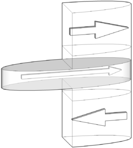
A penta-layer MTJ structure with only a half-ellipsis used as the reference layers (Figure 8.7) is investigated. The geometry
of the device is a similar to that used in the previous section, namely CoFeB(20nm)/MgO(1nm)/CoFeB(3.5nm)/MgO(1nm)/
CoFeB(20nm).
Figure 8.8 shows the oscillating process in such a structure in details. It was found that the structure with half-elliptic
pinned layers, in contrast to the standard structure with the elliptic pinned layers, shows stable oscillations with nearly
constant amplitude. The Fourier transform of the signal is sharply peaked around the frequency ~6.785GHz
(Figure 8.9a).
The frequency of the oscillations only slightly depends on the current densities, as shown in Figure 8.9b.
8.2.2 Two MTJs with shared free layer
Unfortunately the structure with half-elliptic reference layer proposed in the previous section, has one major drawback,
namely a narrow range of current densities at which the oscillations are observed, which limits its use. This is due to the
fact that despite the partial coverage of the free layer by the reference layers, resulting in the spin-current
injection in only a part of the free layer, the free layer magnetization switching may still occur at higher
currents.
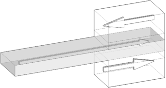
In order to demonstrate this fact more clearly, the system consisting of CoFeB(5nm)/
MgO(1nm)/CoFeB(3.5nm)/MgO(1nm)/CoFeB(5nm) MTJs, with the reference layers 20 × 10nm2 (a × b) and rectangular
free layer 70 × 10nm2 (Figure 8.10, left) is considered. Figure 8.10 (right) shows the dynamics of the magnetization
component along the x-direction of the long axis as a function of time. The current density used for switching
is equal to 1 ⋅ 107A/cm2. Despite that the fixed layer covers only a part of the free layer, so the injection
of spin-current occurs in a part of the free layer only 20nm long, it is still possible to switch the free layer
magnetization.
For demonstration of the switching process the magnetization dynamics of the free layer at different instances is shown in
Figure 8.11. One can conclude that after applying the current a transversal domain wall is formed in the free magnetic layer
close to the area of the spin-current injection, the motion of which away from the MTJ eventually switches the free
layer.
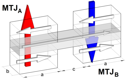
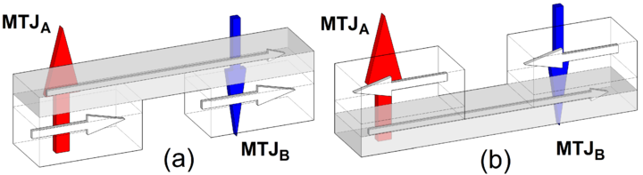
In order to prevent the switching of the free layer and to favor an oscillatory behavior, a second MgO-MTJ is added to
the system (Figure 8.12).
First, the system with the free layer of a rectangular form with dimensions 50 × 10nm2 (c=10nm), and the reference layer
sizes to be the same as in the previous simulations (20 × 10nm2) is examined. The current density through the MTJA is
7.5 ⋅ 107 A/cm2 and 1 ⋅ 107 A/cm2 through the MTJB. Figure 8.13 shows the switching process in such a structure in detail.
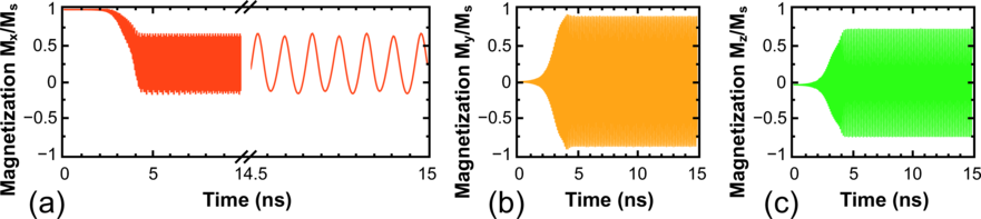
It is found that, in contrast to the previously considered structure, the structure with the two MgO-MTJs demonstrates
stable oscillations with a constant amplitude. The Fourier transform of the signal is sharply peaked around the frequency of
13GHz (Figure 8.14).
In order to understand the oscillations in such structures, the dynamics of the magnetization in MTJB in the pseudo
macro-spin approximation (Figure 8.15) is considered. The pseudo macro-spin approximation includes the following actions:
(i) the modeling of the magnetization dynamics was originally made as micromagnetic simulation; (ii) for MTJB the
magnetization at each time is averaged over the area of MTJB.
As can be seen, the cause of the high-frequency of oscillations in such structures, as compared with other structures that
are experiencing oscillation without an external field, is that during each cycle the magnetization passes twice through the
magnetization states with opposite direction.
Geometrical dependence of the oscillation regime appearance
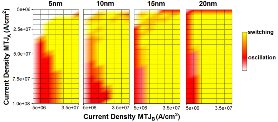
One of the important issues for future practical applications of this concept of oscillators is finding the conditions under
which the transition between the oscillating behavior to the complete switching occurs. To clarify this issue, the structures
with free layer length from 45nm to 60nm (with 5nm step), and width equals to 10nm are investigated. The current density
through the MTJA is from 5 ⋅ 106 A/cm2 to 1 ⋅ 108 A/cm2 and from 5 ⋅ 106 A/cm2 to 3.5 ⋅ 107 A/cm2 through the
MTJB.
The results (Figure 8.16) indicate that increasing the length of the free layer and thus the distance between the
MgO-MTJs shifts the oscillation region towards larger ja∕jb ratio. The white area in Figure 8.16 means that none of
the types of behavior during the simulation time (15ns) was observed and the system presented its initial
state.
The influence of current density and geometry on the oscillation frequency
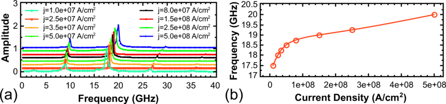
Next, the influence of the current density ja∕jb ratio on the oscillation frequency is studied. The structures with geometry of
the free layer 60 × 10nm2 (c=20nm) are examined. The current density through the MTJA varies from 1 ⋅ 107 to 5 ⋅ 108
A/cm2, while in MTJB it is fixed to 5 ⋅ 106 A/cm2. The simulation results shown (Figure 8.17), that increasing the ratio
ja∕jb increases the oscillation frequency.
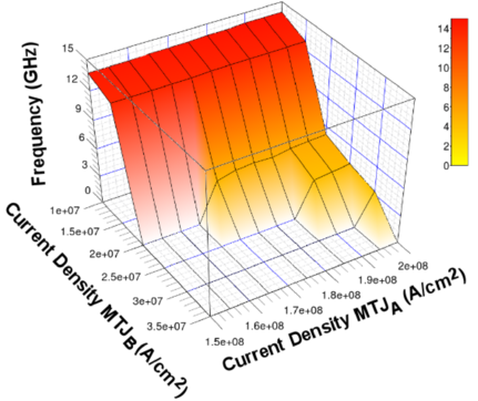
Now the structures with a geometry of the free layer 50 × 10nm2 (c=10nm) are investigated. The current
densities through the MTJA vary from 1.5 ⋅ 108 to 2 ⋅ 108 A/cm2, while through the MTJB from 1 ⋅ 107 to
3.5 ⋅ 107 A/cm2. Increasing j
a leads to an increase of the range of jb, where the stable oscillations are observed
(Figure 8.18).
The output power depends on the oscillations amplitude (mxmax -mxmin)∕2, as it directly reflects the difference between
the two extremes in the magnetization oscillations.
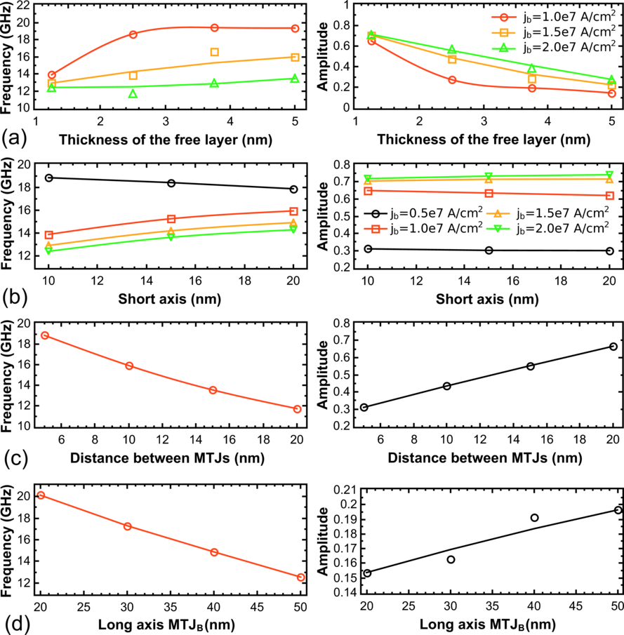
Figure 8.19 shows the simulation results for frequency and amplitude of the oscillations for different geometrical
parameters: thickness of the free layer, short axis, distance between the MTJs, MTJB long axis. The simulations
demonstrate that a decrease of the distance c between the MTJA and MTJB, a decrease of the long axis a of the MTJB,
and an increase of the short axis b and thicknesses of the free layer cause an increase of the frequency at the same current
density. The oscillation amplitude depends on the geometry in the manner inverse to that of the frequency, except the
variation of the short axis b and thicknesses of the free layer, which do not lead to noticeable changes in the amplitude of the
oscillations. It is to note, that the variation of the long axis of the MTJA does not lead to a change in the frequency and
amplitude of oscillations.
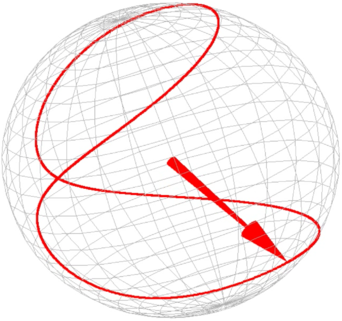
Structure optimization of the spin-torque oscillator
Using the simple dependences derived in the previous section showed that the structure of the free layer 45 × 10 × 1.25nm3
combines both high frequency and amplitude of oscillations (Figure 8.20). The current density through the
MTJA is 5 ⋅ 108A/cm2 and 2 ⋅ 107A/cm2 through MTJB. The transition to the oscillation regime required less
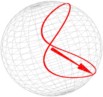
than 1ns. Figure 8.21 shows oscillation trajectory in the MTJB of this structure in the pseudo macro-spin
approximation.
In what follows, the oscillations in a system composed of two three-layer MgO-MTJs with a shared free layer
(Figure 8.22) are investigated. The structure geometry and the current densities are the same as for the previous
oscillator.
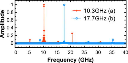
Both structures based on two three-layer MgO-MTJs with shared free layer (Figure 8.22a and Figure 8.22b), as well as
structure based on two penta-layer MgO-MTJs (Figure 8.12), demonstrate stable oscillations. Figure 8.23 shows the signal
spectral density normalized to its maximum value. The peaks of the amplitude are observed at the frequencies of 10.3GHz
and 17.7GHz for the structure (a) and (b), respectively. Note that the structure (b) shows an oscillation frequency higher
than the conventional penta-layer structures and three-layer (a) at the same current densities. The reason
is the in-plane magnetic field due to the pinned layers. In contrast to the conventional penta-layer MTJ,
where the magnetostatic field is compensated, in the three-layer MTJ structure this field tries to reverse the
magnetization in the structure (a) or to stabilize it in the structure (b). This results in an increase (decrease) of the
operation frequency in the structure (b) (structure(a)) as compared to the conventional structure based on two
penta-layer MgO-MTJs, making these structures attractive for tuning their frequency without biasing magnetic
field.