 |
The preprocessor laygrid [68] was designed for simple manually edited three-dimensional solid modeling. Besides solid modeling it can generate tetrahedral grids suitable to be used with finite-element simulators. It works based on a layered description, where a complete structure is created by stacking planar layers (that are associated with some thickness).
Each layer is made of faces with contacts (specifying net names and external voltage/current conditions) and material references. The faces (in X-Y plane) correspond to the top view of the structure to be built at a given z-coordinate. The coordinates of faces were initially entered by hand, so this method was applicable only to very simple structures, made of not more than a few wires. Yet, as they relate to the lateral features, it becomes obvious that the same tool could use the layout to automatically determine the face coordinates. Only the thickness of each layer must be additionally given. The net-names and contact attributes are also supplied by the layout. Thus, the error prone face coordinates specification is replaced by layout edition, the most natural and intuitive manner of representing device and interconnection wire geometries of an integrated circuit.
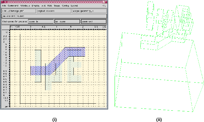 |
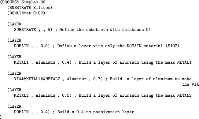
Figure 6.6 presents an example of the
auxiliary file (or process file) used with
the layout information to build a layered solid model of the first two metal
interconnect levels of an integrated circuit. We start by defining the substrate
material (optional) that is used to build the initial (bottom) layer of the
structure (usually made of silicon) and the domain material that is the default
material in the subsequent layers (typically SiO![]() ). Both substrate and
domain materials will have the overall external dimensions of the domain of
simulation specified in the layout and all layout layers must be within this
area.
). Both substrate and
domain materials will have the overall external dimensions of the domain of
simulation specified in the layout and all layout layers must be within this
area.
An advantage of using this layout based approach of solid modeling is the possibility of easily generating parameterized sets of structures. The user has only to write the process file and utilize the automatically parameterized layout set generation tool described in Section 3.3. Naturally, if the thickness of the layers is also to be varied, several of these files need to be created, but this is a much simpler task than calculating all the faces coordinates.
Another advantage is gained at complex structures with many circuit nodes as it is almost impossible, by hand, to keep tracking of the correct node name of each face. As net-names can be assigned automatically at the layout level for each node, this problem is implicitly solved. The same considerations apply to contact pairs needed for resistance extraction. For more accurate lumped model extraction, auxiliary contacts are automatically generated at points where the interconnect wires split in two or more paths. The result of this method used with the layout of the Institute for Microelectronics logo and the previously presented process file is given in Figure 6.7.