


Next: 5.4 SPICE Modeling Interface
Up: 5. Implementation
Previous: 5.2 Process Flow Interface
Subsections
A typical test-chip architecture demands numerous repetitions of the same
test device with only slightly varied parameters. Traditionally the development
engineer specifies the devices needed and documents their parameters. Based on
this documentation the layouter draws the test structures and a test engineer
creates test programs for an automated parameter tester. The large amount of test
structures as, e.g., seen in a typical CMOS based high voltage process demands
the need for an automated one-source template based system to create layout,
documentation, and test programs. This system itself has to be flexible enough
to allow easy incorporation of new test structures and measurement methods.
The development engineer creates one master file defining a set of
test structures and parameter variations (such as e.g. well distance
variations). In this file one can also define the measurements to
be performed, using a simple meta-syntax. A script that uses a predefined
cell library to create the layout of test lines with a standardized pad layout
reads this file. The test lines are arranged and placed in the test chip
automatically, and the exact position of these lines is provided to the
automatic test system. A second script uses measurement templates to convert
the master file in test programs suitable for the specific test system. The
resulting layout files and test programs are hyper-linked into the
documentation that can be used as a reference by the development engineer fur further
analysis. An overview about this scheme is shown in
Figure 5.3.
Figure 5.3:
Electrical test program
conversion work-flow
|
|
The modules involved in creating the test programs for the electrical
parameter extraction use several layers of abstraction.
On the lowest level there are the test routines for parameter extraction
itself, e.g., a threshold voltage extraction or a breakdown voltage extraction
routine. These routines contain all the instrument specific commands and
calculations that are necessary to obtain device parameters. The routines can
make use of a fairly large number of parameters specifying everything up to
delay times, integration times, and compliance values (see
Table 5.1).
Table 5.1:
Parameters for threshold measurement routine
| Parameter |
Comment |
Parameter |
Comment |
| Gate |
Gate pins |
Idcpl |
Compliance for drain current |
| Drain |
Drain pins |
Vsubsforce |
Optional substrate bias |
| Source |
Source pins |
Isubcpl |
Substrate current compliance |
| Substrate |
Substrate pins |
Dtime |
Settling time before |
|
|
|
measurement is taken |
| Type |
Specifies NMOS or PMOS |
Strategy |
Measurement strategy. |
|
|
|
Supported strategies are |
|
|
|
measure, integrate and average |
| Idstart |
Minimum drain current to |
Stepno |
For strategy average: |
|
start drain voltage sweep |
|
number of points to average |
| Vdsstep |
Step width of |
Steptime |
For strategy average: |
|
drain voltage sweep |
|
time interval between |
|
|
|
measurements |
| Vdspoints |
No. of points for |
Vtsmeas |
Return value: |
|
drain voltage sweep |
|
measured threshold voltage |
| Vdscpl |
Compliance for drain voltage |
|
|
|
However, in most cases the test program designer does not want to care about
all these details, but wants to use a simple routine where one specifies the
pads to use and some basic parameters specific to the DUT. Therefore a set of
templates was introduced to provide a translation from an easy-to-use
syntax to the more powerful but also more complicated measurement routine
syntax (see Listing 5.4).
![\begin{lstlisting}[float=tbp, frame=shadowbox,caption={Template definition},
la...
...
</Design_Rule>
<Result>
ILEAK[pA]
BV[V]
S[um]
DR[um]
</Result>
\end{lstlisting}](img191.png)
These templates also make it possible to have several measurement commands
call the same routine with different parameters. Thereby one may specify
measurements with different current compliance values or settling times for
different types of transistors.
The development engineer does not need to deal with the specific parameter set for
every basic routine. If the actual templates are not sufficient for the task
needed, the specialist responsible for electrical test can provide a
new template.
A test program in the development engineers' view consists of the following parts (see
Listing 5.5).
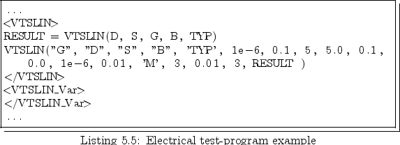
- A header specifying the name of the test-line and thus the position of
the line in the floor-plan
- Some global parameters for the whole test-line
- A list of devices specifying the associated pins and specific device
information, such as geometric parameters
- A set of measurement instructions to be performed on each device in the
line
- An optional set of instructions to be performed after the
measurements. This block is intended for doing calculations on the measured
parameters, such as extracting design rule parameters
This configuration offers the flexibility to define programs for design
rule test-chips and similar test-chips consisting of test-lines with only similar
devices. However, the test program has to be defined manually for each test
line.
For a recent high voltage process development project the evaluation of
geometric variations of high voltage transistors was needed. Because of the
fact that these transistors have a rather complex layout and therefore a lot
of layout parameters that modify the transistor behavior, the testchip turned
out to include up to 1536 similar devices to be layouted in up to 129 test
lines. In total there have been 466 test lines with only 7 different types of
transistors. In order to rule out human errors and make life easier for designers and
test program developers, it was crucial to automate as much work as possible.
As input only some basic device layout and tables were needed, to specify
which parameters to vary in what sequence. From these input files the layout
and arrangement of the devices on the test lines was performed automatically. The
resulting arrangement list was used as an input for a script that used a
general template measurement program similar to
Listing 5.4 and filled up the <NAME> and
<PIN_TABLE> section with the correct information. This configuration
only requires the seven template files to be created and guarantees that all
test lines are measured in the same way.
The resulting program definition files are converted into test programs for
the test system. In addition the layout scripts create a
coordinate list for the test lines, so that these coordinates can be appended
to the wafer definition required by the test system.
The whole test-chip is documented in HTML format by a table of test lines, each
of which has a link to the layout and to the test program definition
file. This documentation is also created from the arrangement list resulting
from the transistor variation, and from a manually created arrangement list
with those design rule structures that are only available on single test
lines. However, the conversion to HTML is performed with a script and therefore is
not prone to human errors.
The creation and the maintenance of test programs for design rule and device
evaluation test-chips has been drastically facilitated by the introduction of
an automated test program creation suite. The time to create a test program
for device screening could be reduced from several weeks when the programs
would have been created manually to a few days for the initial working
templates. Any changes in the measurement sequence could be done within hours
instead of weeks. It was guaranteed also, that all devices were measured
in the same way without the risk of typing errors in the measurement programs.
Next: 5.4 SPICE Modeling Interface
Up: 5. Implementation
Previous: 5.2 Process Flow Interface
R. Minixhofer: Integrating Technology Simulation
into the Semiconductor Manufacturing Environment
![\includegraphics[angle=0,origin=c,width=0.5\textwidth,clip=true]{figures/automated_test_creation.ps}](img190.png)