Next: 3.3.3 Bandgap Narrowing
Up: 3.3 Band-Structure
Previous: 3.3.1 Bandgap Energy
3.3.2 Bandgap Offsets
The problem to align the bandgaps of two or more different materials is old and
not completely solved [129,130,131] due to the
dependence on the growth conditions. The many suggested approaches mainly
differ in whether to use the electron affinity to align the conduction bands,
whether to align the midgaps, or whether to align the valence band edges. In
MINIMOS-NT the last approach is used.
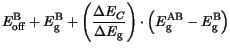
An energy offset,
 , is used to align the band edge energies of different
materials.
is an arbitrary value and by changing it consistently for
all materials at the same time the same results are obtained. As a default in
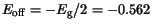
MINIMOS-NT for the group IV materials the reference material is Si. The origin of
the energy axis is assumed to be in the middle of the Si bandgap at 300 K. This
corresponds to a fixed value for Si of
, is used to align the band edge energies of different
materials.
is an arbitrary value and by changing it consistently for
all materials at the same time the same results are obtained. As a default in
MINIMOS-NT for the group IV materials the reference material is Si. The origin of
the energy axis is assumed to be in the middle of the Si bandgap at 300 K. This
corresponds to a fixed value for Si of
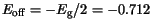
 eV. For the III-V
material system GaAs is chosen as the reference material. Therefore, the offset
for GaAs is
eV. For the III-V
material system GaAs is chosen as the reference material. Therefore, the offset
for GaAs is
 eV. The default offsets for other materials,
summarized in Table 3.14, are chosen to give good agreement with reported data from
[108,111,129,130,131].
eV. The default offsets for other materials,
summarized in Table 3.14, are chosen to give good agreement with reported data from
[108,111,129,130,131].
Table 3.14:
Parameter values for modeling the bandgap energies
| Material |
[eV] |
Material |
[eV] |
| Si |
-0.562 |
InAs |
-0.286 |
| Ge |
-0.157 |
InP |
-0.724 |
| GaAs |
-0.712 |
GaP |
-1.062 |
| AlAs |
-1.008 |
|
|
|
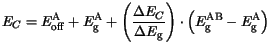
The energies of the conduction and valence band edges
are calculated by
| |
|
 |
(3.66) |
| |
|
 |
(3.67) |
For alloy materials, the following expressions for the conduction and valence band
energies are often used.
| |
|
 |
(3.68) |
| |
|
 |
(3.69) |
The change of the bandgap with the material composition is defined by the ratio
 , starting from one of the materials. For example, for
Al
, starting from one of the materials. For example, for
Al Ga
Ga As/GaAs interface it is known that this ratio equals 60%.
This means that, with increasing
As/GaAs interface it is known that this ratio equals 60%.
This means that, with increasing  , 60% of the increase of the bandgap
(
, 60% of the increase of the bandgap
(
 ) is contributed to the conduction band
(
) is contributed to the conduction band
( ) and 40% to the valence band (
 ). The model, being so
formulated, is not symmetric and general enough. However, assuming
is constant for the whole composition range one obtains:
). The model, being so
formulated, is not symmetric and general enough. However, assuming
is constant for the whole composition range one obtains:
Thus, from (3.68) and (3.70) the ratio
can be expressed as:
Replacing it in (3.68) or (3.70) the offset of alloy material is obtained:
The valence and the conduction band energies are calculated by
(3.66) and (3.67), respectively. Using the default
model parameters in MINIMOS-NT ratios
of 0.12 for
SiGe, 0.6 for AlGaAs, 0.5 for InAlAs,
0.6 for InGaAs, InAsP, GaAsP, and 0.3 for
InGaP are obtained, which are in fairly good agreement with
experimental data [110,89,111,108,132].
The complete bandgap alignment of all semiconductor materials presented in
MINIMOS-NT is shown in Fig. 3.20.
Figure 3.20:
Bandgaps of all semiconductor materials modeled in MINIMOS-NT:
Reference energies for IV group and III-V group materials are the mid gaps of
Si and GaAs, respectively, placed at 0 eV.
|
|
Special attention is paid to the band offsets at the heterointerfaces and
thermionic emission or thermionic-field emission model must be used in
the case of abrupt heterojunctions (see Section 3.1.6).
Next: 3.3.3 Bandgap Narrowing
Up: 3.3 Band-Structure
Previous: 3.3.1 Bandgap Energy
Vassil Palankovski
2001-02-28

![\resizebox{1.18\halflength}{!}{
\includegraphics[width=1.18\halflength]{figs/CbeBand2.eps}}](img368.gif)