


Next: 3.3.4 Effective Carrier Mass
Up: 3.3 Band-Structure
Previous: 3.3.2 Bandgap Offsets
Subsections
3.3.3 Bandgap Narrowing
Bandgap narrowing (BGN) is one of the crucial heavy-doping effects to be
considered for bipolar devices. In MINIMOS-NT the use of BGN model is optional.
The model of Slotboom
[133] is widely used in case of silicon.
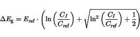 |
(3.73) |
The shifts of the conduction and valence band edges are calculated by
 gives the part of the total BGN
 which is
contributed to the conduction band. The default parameter values are
summarized in the following table.
which is
contributed to the conduction band. The default parameter values are
summarized in the following table.
Table 3.15:
Parameter values for modeling the bandgap narrowing
| Material |
 [eV] [eV] |
 [cm [cm ] ] |
|
| Si |
0.009 |
1e17 |
0.5 |
|
Using the physically-based approach from [93], a new analytical BGN
model was developed. It is applicable to compound semiconductors
[134] and considers the semiconductor material and the dopant species
for arbitrary finite temperatures. In this section a comparison with
experimental data and other existing models is presented and study of BGN in
III-V group semiconductors is performed.
Despite of many papers dedicated on BGN in semiconductors, the optimal
balance between accuracy of the results and simplicity of model implementation
seems had not been achieved. Commercial device simulators, such as
ATLAS [50] , DESSIS [40], and MEDICI [41], use the
logarithmic fit models for BGN in Si from [133,135,136,137] which
are simple to implement, but deliver non-physical values below and above definite
doping levels.
Furthermore, the functional form of models for Si is used for models for other
materials (e.g. III-V compounds [138]) or the BGN effect is left
completely ignored. Comparisons of these models are shown in
Fig. 3.21. The physical limit our model offers (0 meV for undoped
materials), the physically sound explanation of some existing effects it gives,
the ability to treat various semiconductor materials and dopants, and the
simplicity of the model, make it very applicable for device simulation
purposes.
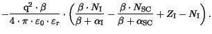
The basic assumption in our model is that BGN is a result of five types of
many-body interactions (electron-electron, electron-impurity, hole-hole,
hole-impurity, and electron-hole). The electron-impurity contribution is
assumed to be dominant at high doping concentrations. Though BGN is very
difficult to model rigorously due to multiple carrier interactions one can
approximate the energy shift to first order by the classical self-energy of the
electron in the field of an ionized impurity [93]. Thus one obtains
Here
 and
and  denote the screened and unscreened
Coulomb potentials of the impurity, respectively. (3.76) represents the
change in the electrostatic energy of the impurity before and after the
electron gas redistribution. If the potential of a point-like impurity is
assumed, the Fourier transform of the scattering potential is expressed by
(3.78), where
denote the screened and unscreened
Coulomb potentials of the impurity, respectively. (3.76) represents the
change in the electrostatic energy of the impurity before and after the
electron gas redistribution. If the potential of a point-like impurity is
assumed, the Fourier transform of the scattering potential is expressed by
(3.78), where  and
and  are the atomic number and the number of
electrons of a given material,
are the atomic number and the number of
electrons of a given material,  denotes the inverse Thomas-Fermi length,
and
denotes the inverse Thomas-Fermi length,
and
 is the Fermi integral of order
  [139]. This
approach leads to a simple BGN model [93] given by (3.80).
[139]. This
approach leads to a simple BGN model [93] given by (3.80).
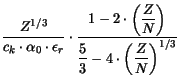
Removing the point-charge approximation yields a refined model. The charge
density of the impurity can be accounted for by an atomic form factor
 . Following the work [140] the impurity potential takes the form
Solving (3.77) using (3.81) and (3.82), and then
replacing V(r) in (3.76), leads to the final expression for the energy shift
The subscripts  and
and  refer to a semiconductor and impurity,
respectively. and are the atomic number and the number of electrons of
a given material.
refer to a semiconductor and impurity,
respectively. and are the atomic number and the number of electrons of
a given material.  can be interpreted as size parameters of the electron
charge density and
can be interpreted as size parameters of the electron
charge density and  is the Bohr radius. They are expressed as
The size parameter uses
 , which is the most pessimistic
estimation, since it is still not clarified which value for
in the
range between 1 and
, which is the most pessimistic
estimation, since it is still not clarified which value for
in the
range between 1 and
 is valid at microscopic level. Even though
the influence of the dopant type is reduced to minimum this way, our model
still delivers appropriate results at 300 K in agreement with experiment
[141] (see Fig. 3.22).
is valid at microscopic level. Even though
the influence of the dopant type is reduced to minimum this way, our model
still delivers appropriate results at 300 K in agreement with experiment
[141] (see Fig. 3.22).
The temperature dependence of the BGN in Si is shown in Fig. 3.23.
Neglecting of the stronger BGN at low temperatures, especially for doping
levels of about  cm, may result in an error of about
50%. Thereby, even larger errors might be introduced into the simulation
results, with respect to the electrical device characteristics. In the case of
III-V semiconductors our model delivers a comparatively weaker BGN temperature
dependence (see Fig. 3.24). Similar observations were reported in the case of
p-GaAs in [142], [143]. Thus, according to our knowledge, our BGN
model is the first theoretically derived model predicting different shifts for
various dopant species and taking temperature into account.
cm, may result in an error of about
50%. Thereby, even larger errors might be introduced into the simulation
results, with respect to the electrical device characteristics. In the case of
III-V semiconductors our model delivers a comparatively weaker BGN temperature
dependence (see Fig. 3.24). Similar observations were reported in the case of
p-GaAs in [142], [143]. Thus, according to our knowledge, our BGN
model is the first theoretically derived model predicting different shifts for
various dopant species and taking temperature into account.
Figure 3.21:
Comparison with models used in other device simulators
|
|
Figure 3.22:
Influence of the dopant material on BGN in n-Si
|
|
Figure 3.23:
Temperature dependence of the bandgap narrowing in n-Si
|
|
Figure 3.24:
Temperature dependence of the bandgap narrowing in n-GaAs
|
|
Figure 3.25:
Influence of the dopant material and material
composition in p-Si and p-SiGe
|
|
Figure 3.26:
Ge-content dependence in p-SiGe compared to experimental data
|
|
Figure 3.27:
BGN in GaAs compared to experimental data
|
|
Figure 3.28:
BGN for various n-type binary compounds
|
|
The model extends its validity also for alloy semiconductors by material
composition dependent relative effective masses for electrons and holes, on the
one hand, and permittivity, on the other hand.
In Fig. 3.25 the results for boron and gallium doped Si Ge
Ge for
different Ge contents are presented. This is even better illustrated in
Fig. 3.26 where the BGN versus material composition in SiGe is
compared to another model proposed by Jain and Roulston
[144] suggesting increased BGN. The decrease of the BGN with increase of
the Ge fraction was already experimentally observed in [145],
[146]. Our theoretical approach explains this effect by the decreased
valence band density of states and increase of the relative permittivity in the
SiGe alloy.
for
different Ge contents are presented. This is even better illustrated in
Fig. 3.26 where the BGN versus material composition in SiGe is
compared to another model proposed by Jain and Roulston
[144] suggesting increased BGN. The decrease of the BGN with increase of
the Ge fraction was already experimentally observed in [145],
[146]. Our theoretical approach explains this effect by the decreased
valence band density of states and increase of the relative permittivity in the
SiGe alloy.
In the case of p-type GaAs good agreement with experimental data
[142], [143] is obtained. The few available experimental data for n-type GaAs
suggest sometimes lower [147] (open triangles in Fig. 3.27) values for BGN
and more often higher [148] (filled triangles) than our model
delivers. This confirms the importance of modeling BGN in III-V semiconductors,
instead of leaving this effect unconsidered, which is the case with most device
simulators.
Experiments showed higher BGN in n-InP than in n-GaAs [149]. Higher
conduction band density of states and lower relative permittivity explain the
expected higher values for BGN in AlAs and GaP (Fig. 3.28) than in InP, GaAs,
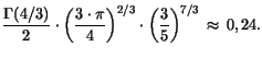
and InAs. The parameter values are taken from [108]. The model is
physics-based and contains no free parameters except the ratio
used in (3.74).
Next: 3.3.4 Effective Carrier Mass
Up: 3.3 Band-Structure
Previous: 3.3.2 Bandgap Offsets
Vassil Palankovski
2001-02-28


![\resizebox{\halflength}{!}{
\includegraphics[width=\halflength]{figs/CbgnSi1.eps}}](img405.gif)
![\resizebox{\halflength}{!}{
\includegraphics[width=\halflength]{figs/CbgnSi2.eps}}](img406.gif)
![\resizebox{\halflength}{!}{
\includegraphics[width=\halflength]{figs/CBWbgnSiT.eps}}](img407.gif)
![\resizebox{\halflength}{!}{
\includegraphics[width=\halflength]{figs/CBWbgnGaAsT.eps}}](img408.gif)
![\resizebox{\halflength}{!}{
\includegraphics[width=\halflength]{figs/CBWbgnSiGen.eps}}](img409.gif)
![\resizebox{\halflength}{!}{
\includegraphics[width=\halflength]{figs/CbgnSiGex.eps}}](img410.gif)
![\resizebox{\halflength}{!}{
\includegraphics[width=\halflength]{figs/Cbgngaaspn.eps}}](img411.gif)
![\resizebox{\halflength}{!}{
\includegraphics[width=\halflength]{figs/Cbgn35.eps}}](img412.gif)