As mentioned above, process and device simulation often provide the
only means of looking into the semiconductor material to determine the
distribution of physical quantities like dopant concentration or
carrier density. Given a ``real'' device, one can combine these
techniques to indirectly measure two-dimensional dopant
profiles by matching electrical measurements obtained from experiments and simulation
[Kha95] [KFBS95].
Figure 2.6 shows the optimization loop identifying
a doping profile by means of electrical device characterization and
inverse modeling.
by matching electrical measurements obtained from experiments and simulation
[Kha95] [KFBS95].
Figure 2.6 shows the optimization loop identifying
a doping profile by means of electrical device characterization and
inverse modeling.
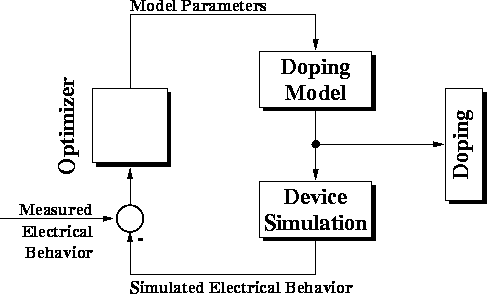
Figure 2.6: Inverse modeling of doping profile.
Given a parameterized model of the doping profile, an optimizer tries to minimize the deviation of the simulated device parameters from measured data by adjusting the parameters of the doping model. The model may be an implantation simulator, a sequence of process simulation tools, or an analytical model of the doping profile. In the latter case, care has to be taken not to introduce false or unjustified assumptions on the nature of the solution sought.