The interface between device design and process simulation is based on lithography mask data that are either specified as numerical coordinates or derived directly from the device layout. For two-dimensional simulation, mask coordinates define a one-dimensional sequence of transparent and dark areas. Figure 5.9 shows a two-dimensional cross-section of the wafer with the one-dimensional lithography mask cross-section defining the poly-silicon gate atop the gate oxide layer during exposure and after removing the exposed photo resist and etching the poly-silicon not covered by photo resist.
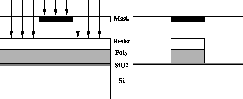
Figure 5.9:
Two-dimensional wafer cross-section and
one-dimensional lithography mask cross-section during exposure
and after etching the poly-silicon layer.
Cut-lines and cross-sections for defining simulation areas are specified
in an integrated layout editor [MS96] based
on the PIF editor [RHS95] [Rie96] Figure 5.10 gives an overview of the generation of one-dimensional mask
data from layout data imported either from a ECAD system or
entered manually by the user using the PIF editor.
Figure 5.10 gives an overview of the generation of one-dimensional mask
data from layout data imported either from a ECAD system or
entered manually by the user using the PIF editor.
The one-dimensional mask file is used in process simulation to define mask coordinates at lithography steps in the process flow. Lithography masks are specified by name, boolean operations are used to to define a location on the wafer surface as a function of various mask geometries.
