


Next: 5.2.1 Producing a Device
Up: 5. Building Simulation Models
Previous: 5.1.5.1 Semiconductor Wafer Descriptions
Similar to the simulation of fabrication processes, the simulation-flow-model
can be applied to encapsulate simulators which model the electrical
behavior of a semiconductor device. We will demonstrate in the
following how this can actually be done by building a simulation-flow-model
based on the MINIMOS-NT device simulator. Example 5.4
depicts this simulation-flow-model which encapsulates and controls the
MINIMOS-NT device simulator. The input port named device defines
the semiconductor device to be investigated by
MINIMOS-NT. Example 5.5 lists the input deck template used to
control MINIMOS-NT.
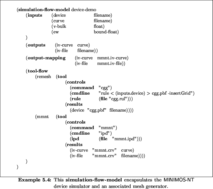
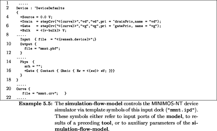
We use a template symbol named curve to
define a file which tells MINIMOS-NT the sequence of operating points it
should compute in order to produce an I/V-curve. The value for this
symbol comes from the input port of the simulation-flow-model. Instead of
defining an I/V-Curve we could also create template symbols which
simply define the electrical potential at various electrical contacts
of the device and associate these contacts with ports of the
simulation-flow-model, like this is done for the bulk contact.
Next: 5.2.1 Producing a Device
Up: 5. Building Simulation Models
Previous: 5.1.5.1 Semiconductor Wafer Descriptions
Rudi Strasser
1999-05-27