Point defects in solids have been in the focus of scientific interest since the very beginnings of solid state theory due to their large influence on the macroscopic mechanical, electrical, and optical properties of the host material. In semiconductor technology, which is itself largely based on the intentional introduction of impurities into a host material, defects affect the motion of the electrons and the holes by scattering, carrier trapping, or as recombination centers. Under certain operational or environmental conditions, or just over time, point defects in a given semiconductor device might be created, destroyed, repositioned, or modified in their ability to interact with the carriers. As these changes usually alter the characteristics of the device in an undesired manner, detailed knowledge of the defect physics is of utmost importance in the field of semiconductor device reliability, within which the present work has been carried out.
| Figure 1.1: | Schematic of a typical BTI measurement. During stress, a large negative gate voltage V g is applied. The degradation is monitored through the drain current which is driven by applying a small voltage along the channel. |
The main focus of interest for this thesis lies in the bias temperature instability (BTI) of
metal-oxide-semiconductor (MOS) transistors. This instability is usually encountered during burn-in
tests or high-performance operation of MOS devices [1, 2] at temperatures in the 100
Lifetime predictions for BT instabilities are usually made based on accelerated (so-called burn-in)
tests, where the devices are operated at temperatures and voltages that are beyond their
specifications, aiming at the amplification of one specific degradation mechanism as much as
possible without damaging the device otherwise. The degradation observed in these tests
is then extrapolated to the normal operation conditions by using empirical
In order to obtain accurate long-term (ten years or more) predictions for the amount of
degradation induced by a certain mechanism, a detailed physical understanding of this
degradation process is required. The identification of the relevant physics, however, proves to
be difficult in practice due to the limited experimental observability. These limitations
arise from the small structural dimensions of the microelectronic devices together with the
low density of defects present in the materials. The resulting number of defects generated
during stress in a commercial device is below the detection limit of most measurement
methods that give hints to the atomic structure involved, like electron spin resonance (ESR,
also known as electron
| Figure 1.2: | The
basic
concept
behind
the
reaction-diffusion
model
for
NBTI.
( |
| …silicon …oxygen |
| …hydrogen |
Because of its impact, most modeling has been done on the
During stress, the presence of holes at the interface and the increased temperature leads to a
liberation of the hydrogen atoms. The remaining silicon dangling bonds become electrically active
carrier traps. According to the model, the depassivation and repassivation of dangling bonds at the
interface reaches an equilibrium in a very short time [8, 9], and it is the constant flux of hydrogen
atoms (or some hydrogenic species) away from the interface that determines the temporal evolution of
the degradation. Because of the two proposed stages — the electrochemical reaction at the interface
and the subsequent diffusion of the hydrogenic species — this model bears the name
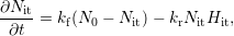
The mathematical framework the of model is based on a macroscopic description using a rate
equation for the interface reaction and a Fickian diffusion equation for the motion of the hydrogen in
the oxide. Central actors are the density of depassivated silicon dangling bonds at the interface
|
| (1.1) |
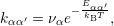
with the depassivation (forward) rate
 = =  | (1.2) |
 | (1.3) |
This power-law degradation corresponded well with experimental results of the seventies.
| Figure 1.3: | Basic features of the degradation
predicted by the RD model for NBTI. In the
initial phase, the depassivation reaction with
rate |
In later experiments, power-law exponents were found that differed from the 1
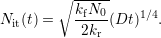
| Figure 1.4: | Typical recovery trace as predicted by the RD model for NBTI using equations (1.4)–(1.6), which is similar for all variants of the RD mechanism. The comparison with experimental data [12] shows that the RD predicted recovery occurs much too late and proceeds much too fast. |
Several extensions to the RD model have been put forward, such as dispersive transport of the
hydrogenic species [11, 9], but none could give the observed experimental behavior. The current
state-of-the-art RD-based modeling supplements the RD theory with empirical hole-trapping
expressions. It is assumed that short-time (1s) degradation and recovery is dominated by hole trapping
into oxide and interface defects, while the long-term degradation and recovery are determined by
the RD mechanism [15, 16, 17, 18]. The RD theory employed in these modeling efforts
is the
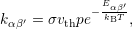
 | = | (1.4) |
 | =  | (1.5) |
 | =  + +   | (1.6) |
The combination of this modified reaction-diffusion model with empirical hole-trapping somewhat improves the match with experimental DC and AC stress data. The failure of the RD model to properly describe NBT recovery is shifted out of the time window of some experiments, but essentially remains.
Most recently, it has been argued that the shortcoming of the reaction-diffusion based model
concerning the prediction of NBTI recovery comes from the one-dimensional description of the H and
H
We have also derived and implemented a microscopic formulation of the RD model [24, 25], in order to study the behavior of the RD mechanism on the atomic scale. Our calculations, which are more deeply explained in Chap. 3, have disproved the claims in [16, 17] and raise strong doubts of the validity of the proposed RD mechanism and its modeling using rate equations.
| Figure 1.5: | In
the
neutral
oxygen
vacancy,
a
strong
bond
is
formed
between
the
two
silicon
atoms
adjacent
to
the
vacancy.
Upon
hole
capture,
this
bond
is
weakened
and
the
defect
eventually
relaxes
to
the
energetically
more
favorable
‘puckered’
configuration.
The
charged
dimer
position
is
usually
identified
with
the
|
The obvious inability of the reaction-diffusion model and its variants to accurately predict NBTI
recovery as well as other properties, such as the universal scaling of BTI degradation [27], led to
increased interest in alternative descriptions. A promising approach was found in 2008 in BTI models
based on dispersive reactions between two or three states [27, 28], termed double-well or triple-well
models. Although the central actors were still believed to be hydrogen atoms, these models brought a
fundamental reinterpretation of the physical process behind the BTI. The collective diffusion process
that determines the degradation and recovery in the RD models was replaced with a dispersive
hopping of isolated particles. Even better accordance with experimental data was found later that year
with a model that coupled a two-state description of the ‘hydrogen atom’ with an also
statistically distributed thermally activated hole capture process [29]. The introduction of
more complex experimental techniques such as rapid gate voltage and device temperature
switches created new testing-grounds for BTI modeling. Early 2009 a refined model could be
devised that was also able to explain the more complex experimental data with striking
accuracy [26]. This model brought along a complete reinterpretation of the degradation
process that no longer assumes the hole capture to happen at the Si-SiO
While the microscopic picture behind the two-stage model was based on a broad and rigorous literature study, the mathematical description was formulated in a way that only captures the basic behavior arising from the microscopic theories but that did not fully implement the physical details of those theories.
|  |
| Figure 1.6: |
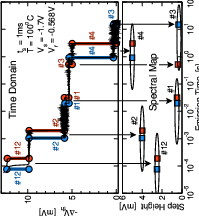
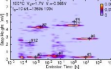
A further advance of the defect model was stimulated by experiments taken on small-area devices, where the recovery in response to NBT stress proceeds in discrete steps instead of a continuous curve [31]. The careful analysis of these steps led to the development of the time-dependent defect spectroscopy (TDDS) method [31, 32, 33], which makes a detailed investigation of the charging and discharging of single defects possible [32]. A typical TDDS spectral map is given in Fig. 1.6. The results of the TDDS experiments served as a testing ground of unprecedented detail for BTI models and allowed for the refinement of the physics in the two-stage model. The resulting multi-state defect model not only fits experimental data from BTI and TDDS experiments very well, it also links these phenomena to other phenomena such as random telegraph noise (RTN) and flicker noise [34, 35, 36, 32, 37].
| Figure 1.7: | |
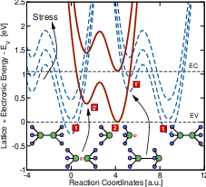
As an extension to the original two-stage model, the multi-state NMP model considers four states of the oxygen vacancy, as illustrated in Figures 1.5 and 1.7, and rests upon a more detailed physical theory for the hole capture and emission rates, which will be more deeply discussed later.
The mathematical formulation of the defect based model assigns a probability
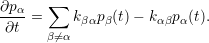 | (1.7) |
The transient behavior of a defect arises from the potential energy surfaces in its various charge states.
The potential energy surface  ) corresponding to a certain charge state
  . In our model, the defect is assumed to have two relevant
potential energy surfaces, corresponding to the neutral and the positive charge state of the defect.
Fig. 1.7 shows the gradual change of the total energies as the system moves in configuration space and
the resulting energetic minima which give rise to the states of the defect (denoted 1, 1
. In our model, the defect is assumed to have two relevant
potential energy surfaces, corresponding to the neutral and the positive charge state of the defect.
Fig. 1.7 shows the gradual change of the total energies as the system moves in configuration space and
the resulting energetic minima which give rise to the states of the defect (denoted 1, 1
 | (1.8) |
where
 | (1.9) |
where
In our model, the defect is initially in state 1, which is electrically neutral. During normal device
operation, the defect will remain there due to the large energetic barriers separating state 1 from all
other states. When large negative bias is applied, the relative energetic shift of the neutral
potential energy surface to the positive ones changes as indicated in Fig. 1.7, resulting in a
decrease of the transition barrier for hole capture from the silicon valence band. After the
transition to the positive state (1
In electrical measurements of large area transistors one observes an ensemble of the described
defects and, due to the amorphous nature of the gate oxide, every defect moves on a different energetic
landscape. This means that all the state energies and barrier energies are statistically distributed
and thus each defect shows a different transient behavior. The macroscopically observed
degradation is the superposition of a large number of defects changing their state from 1 to
2, e.g. due to electrical stress, as the charged state of these defects influence the charge
carriers in the silicon substrate. Similarly, if an increased number of defects undergo the
transition 1
Although the central defect for BTI has been illustrated as an oxygen vacancy up to now, to date
there is no direct experimental evidence of the actual microscopic nature of this defect. Defects in
SiO
Judging from the properties of their ESR-spectra the P
| Figure 1.8: | Schematic illustration of the defects investigated in the present work. |
In addition to oxygen vacancies, also defects involving silicon dangling bonds and hydrogen have
received some attention. Studies showed that atomic hydrogen is produced in quartz under heavy
irradiation conditions [79, 80]. Although hydrogen is routinely used in the production
process of MOS structures to passivate dangling bonds, it has been shown that exposure
to hydrogen can also induce degradation [81, 80, 82]. Particularly interesting for the
present work is the hydrogen-complexed oxygen vacancy, which has been identified with the
E
Unfortunately, electron spin resonance measurements can only give hints on the atomic structure of the defect and electrical measurements can only show the capture and emission behavior of the defects under different operation conditions. Thus from the experimental findings up to this point no conclusion can be drawn regarding the microscopic origin of the BTI. On the modeling side, the great success of the multi-state NMP model for BTI in the explanation of experimental data is somewhat spoiled by the large set of parameters and the unknown defect structure. The model parameters are usually determined by calibration to measurement data. Especially for the modeling of BTI and RTN, however, this method is somewhat unsatisfactory as the measurements show a broad spread in transition rates [34, 87, 31], which requires assumptions on the statistical distribution of the defect parameters. Some insight in the behavior of single defects is gained from the TDDS [31]. However, the measurement of TDDS spectral maps is a quite demanding task and few devices have been analyzed using this technique up to now. Thus, there is not yet enough data available to give an estimate about the statistics of the observed defects.
The goal of the present work is to extend our modeling efforts to the atomic scale, in order to make the prediction of the BTI-related parameters from an atomistic model of a point defect possible. The methods developed and described in this work can be used to evaluate atomistic models of defect candidates against parameters obtained from calibrations to experimental data. In order to find an atomistic model of the BTI defect, different defect candidates can then be evaluated against the available parameter sets. A suitably designed atomistic model of the amorphous MOS oxide could then be used to study the statistics of the BTI defect and make predictions on its stability and its dependence on processing conditions.
At first, we study the foundation of our BTI model in the framework of physical chemistry to get a
detailed understanding of the microscopic processes behind the states and transitions described above.
This includes an attempt to shed some light on the huge amount of literature available for
multi-phonon transitions. In Chap. 4, the microscopic description of the point-defect is put into the
context of a semiconductor device and a multi-scale modeling method is developed, which combines
the description of the defect at the microscopic level with a macroscopic model of the MOS structure.
At the time this document is written, the search for a defect candidate that explains the
behavior seen in BTI experiments is still ongoing. For the reasons stated above, we study the
behavior of atomistic models of the oxygen vacancy and the hydrogen bridge in crystalline
SiO