next up previous contents
Next: 2.4.2 Lower Bound of Up: 2.4 Absolute Lower Bounds Previous: 2.4 Absolute Lower Bounds

2.4.1 Lower Bound of the Supply Voltage

Early work in this field was based on a minimum-inverter-gain criterion, and a minimum supply voltage of 200mV was found for inverters operating in weak inversion [76]. 
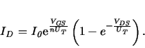
To determine an absolute lower bound of the supply voltage we assume MOSFETs operating completely in the weak inversion mode. The drain current is then given by [A3]

\begin{displaymath}\ensuremath{I_{\mathit{D}}}\xspace = \ensuremath{I_{\mathit...
...DS}}}\xspace }{\ensuremath{U_{\mathit{T}}}\xspace }}} \right).
\end{displaymath} (2.11)

$\ensuremath{I_{\mathit{0}}}\xspace $ is determined by the technology and the channel width-to-length ratio W/L (cf. (A.14)). For the following, we assume also an ideal gate swing of $S = \ln(10) \ensuremath{U_{\mathit{T}}}\xspace $, thus, n = 1. Setting $\ensuremath{I_{\mathit{D,n}}}\xspace + \ensuremath{I_{\mathit{D,p}}}\xspace = 0$ with $\ensuremath{I_{\mathit{0,n}}}\xspace = \ensuremath{I_{\mathit{0,p}}}\xspace $ yields an implicit equation for the transfer curve $\ensuremath{V_{\mathit{out}}}\xspace (\ensuremath{V_{\mathit{in}}}\xspace )$ of a symmetric inverter [63] (see also Section A.2.2.1)

\begin{displaymath}
\frac{\sinh \left( \frac{\ensuremath{V_{\mathit{in}}}\xspace...
...thit{DD}}/2}\xspace }{\ensuremath{U_{\mathit{T}}}\xspace }}}
.
\end{displaymath} (2.12)

To determine the noise immunity of the inverter (cf. Fig. A.6) the critical points where the voltage gain $A = {d\ensuremath{V_{\mathit{out}}}\xspace }/{d\ensuremath{V_{\mathit{in}}}\xspace } = -1$ are determined by

\begin{displaymath}
\frac{2\cosh \left( \frac{\ensuremath{V_{\mathit{in,c}}}\xsp...
...thit{DD}}/2}\xspace }{\ensuremath{U_{\mathit{T}}}\xspace }}}
,
\end{displaymath} (2.13)

from which the noise margins $\ensuremath{{\mathit{NM}}_{\mathit{H}}}\xspace = \ensuremath{{\mathit{NM}}_{\mathit{L}}}\xspace = \ensuremath{{\mathit{NM}}}\xspace $ are computed as

\begin{displaymath}
\ensuremath{{\mathit{NM}}}\xspace = \frac{\ensuremath{V_{\ma...
...t{DD}}}\xspace } \quad [\ensuremath{V_{\mathit{DD}}}\xspace ]
.\end{displaymath} (2.14)

The maximum voltage gain which occurs at $\ensuremath{V_{\mathit{in}}}\xspace = \ensuremath{V_{\mathit{out}}}\xspace = \ensuremath{V_{\mathit{DD}}/2}\xspace $ (cf. (5.1)) is given by

\begin{displaymath}
-\ensuremath{A_{\mathit{max}}}\xspace = {e^{\frac{\ensuremat...
...t{DD}}/2}\xspace }{\ensuremath{U_{\mathit{T}}}\xspace }}} - 1
.\end{displaymath} (2.15)

Solving (2.12) and (2.13) numerically, together with (2.4.1) and (2.15) yields noise margins and maximum gain as a function of the supply voltage. Fig. 2.4 shows a plot of \ensuremath{{\mathit{NM}}} and \ensuremath{A_{\mathit{inv}}} vs. \ensuremath{V_{\mathit{DD}}}.

Figure 2.4: Maximum gain and noise margins of a symmetric inverter with ideal MOS transistorsoperating in weak inversion
\includegraphics[scale=1.1]{dc-perf.eps}

For the design of digital circuits we have to impose certain constraints, i.e., to specify minimum values for $\ensuremath{{\mathit{NM}}}\xspace $ and $\ensuremath{A_{\mathit{max}}}\xspace $ at a nominal and maximum temperature and to estimate the impact of an effective unsymmetry $\ensuremath{F_{\mathit{U}}}\xspace = {\ensuremath{W_{\mathit{n}}}\xspace }/{\ensuremath{W_{\mathit{p}}}\xspace }$ as a consequence of the fan-in of gates in a minimum-transistor-size design. This is accounted for by a shift of the input voltage $\Delta\ensuremath{V_{\mathit{in}}}\xspace = - \ensuremath{U_{\mathit{T}}}\xspace \ln(\ensuremath{F_{\mathit{U}}}\xspace )/2$. Minimum supply voltages for various constraints are compiled in Table 2.2. For static logic with a fan-in of 3 the minimum $\ensuremath{V_{\mathit{DD}}}\xspace $ is 83mV at 300K or 3.22 times the thermal voltage. Note that these numbers are absolute lower bounds which cannot likely be achieved with any CMOS process technology. Achievable values for $\ensuremath{V_{\mathit{DD,min}}}\xspace $ may be estimated by scaling the numbers from Table 2.2 by a factor of $n = S/(\ensuremath{U_{\mathit{T}}}\xspace \ln(10))$ where S is an achievable average gate swing. Although this is not consistent with (2.12) and (2.13), it can be used as a worst-case estimate for subthreshold operation.


Table 2.2: Ideal-case minimum supply voltage \ensuremath{V_{\mathit{DD}}} for given of circuit design constraints
constraint   \ensuremath{V_{\mathit{DD,min}}} \ensuremath{V_{\mathit{DD,min}}}
    ( $T\! = \!\rm 300K$) $[\ensuremath{U_{\mathit{T}}}\xspace ]$
$\ensuremath{A_{\mathit{max}}}\xspace > 1$ (ring osc.) 36mV 1.40
$\ensuremath{{\mathit{NM}}}\xspace > 10\%$ (inverter) 55mV 2.13
$\ensuremath{A_{\mathit{max}}}\xspace > 4$ (std. design) A3mV 3.22
$\ensuremath{F_{\mathit{U}}}\xspace > 9 $ (fan-in = 3) A3mV 3.22
$\ensuremath{I_{\mathit{on}}}\xspace /\ensuremath{I_{\mathit{off}}}\xspace > 10^4 $ (dyn. logic) 238mV B.22


next up previous contents
Next: 2.4.2 Lower Bound of Up: 2.4 Absolute Lower Bounds Previous: 2.4 Absolute Lower Bounds

G. Schrom