As the device feature size continues to be scaled down, increasingly severe requirements are being imposed on plasma etching technology, including the anisotropy of etching, profile control, feature size or CD control relative to the mask width, and etch selectivity to the mask materials and underlying layers [100]. In general, gate etching is a considerable challenge in the fabrication of MOS transistors. In practice, an extremely high etch selectivity of poly-silicon with respect to an ultrathin gate oxide is required for gate etch processes with extremely precise CD control. Furthermore, these requirements must be satisfied for a variety of etched features with greatly differing dimensions or aspect ratios on the wafer.
Microscopic uniformity or aspect ratio dependent etching is one of the most important issues of plasma etching technology [32]. In plasma etching, etch rates and profiles are often observed to depend on pattern feature size or aspect ratios [47], e.g., slower etch rates for features of larger aspect-ratios (reactive ion etching lag) [25], stronger side-wall tapering for features of smaller aspect-ratios [34], more thinning and breaking of gate oxides for features of smaller aspect ratios [13] and vice versa. Such phenomena are generally attributed to a decrease or an increase of incident flux of neutrals onto the bottom surface of an etched feature as the aspect ratio of the feature is increased. It is important to reveal the mechanisms responsible for such microscopic non-uniformities in order to achieve microscopically uniform and aspect ratio independent etching, which in turn results in microscopically uniform channel lengths of the fabricated MOS transistors.
Etching of a poly-silicon gate is frequently performed to achieve anisotropy and selectivity, which are critical as the minimum feature size shrinks. A thorough understanding of the chemical mechanism in ion enhanced plasma etching is required for better process modeling to predict the etching directionality and feature profiles.
Ion-enhanced etching of poly-silicon has been well characterized by many researchers over the last 20-25 years [23,22]. The etching rate can be decomposed into three components [20]: physical sputtering by ions, spontaneous etching by atoms, and ion-enhanced etching which is the combined effect of ion flux, surface coverage, and ion energy.
The decrease of the dimensions of features in IC manufacturing demands more anisotropy, directionality, and compact etching profiles [100,93]. Plasma etching is able to produce highly anisotropic etching profiles. Therefore, it is and will be a very important processing step in IC manufacturing. A better understanding of this important process is crucial for further improvements in this field and for the development of better processing models. In this chapter we will present simulation results for highly anisotropic etching [23].
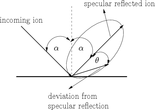
The distribution about the angle of the specular reflection is modeled as
![]() where
where ![]() is the deviation from the angle of
the specular reflection. Obviously higher
is the deviation from the angle of
the specular reflection. Obviously higher ![]() means tighter distribution and
more in the direction of perfect specular reflection. The quantity
means tighter distribution and
more in the direction of perfect specular reflection. The quantity ![]() is called specularity and depends on different parameters such as
surface material, ion mass, ion energy, and ion angle of
incidence. For example, specularity tends to decrease with increasing
ion mass relative to the surface material. As can be seen later in
simulation results the specularity plays an important role in the
prediction of the correct shape and depth of microtrenching.
is called specularity and depends on different parameters such as
surface material, ion mass, ion energy, and ion angle of
incidence. For example, specularity tends to decrease with increasing
ion mass relative to the surface material. As can be seen later in
simulation results the specularity plays an important role in the
prediction of the correct shape and depth of microtrenching.
In the etching process considered, two kinds of neutrals have been assumed:
the first kind are the etchants with ![]() as their flux and the second kind
are the inhibitors with
as their flux and the second kind
are the inhibitors with ![]() as their flux.
as their flux.
Two different sources can be considered for inhibitors. One source is the plasma gas phase. During the etching process volatile etch products will go to the gas phase. If their residence time is long enough, they will produce molecules which can return and stick on the surface of the feature.
The other source for inhibitors is molecules locally produced at the feature during etching. The way these products desorb from the surface depends on the actual etching mechanism.
The best known model for etching kinetics is the Langmuir adsorption model [1,99,47] which gives the following equations
Equalizing the surface coverages to zero is based on the fact that the surface coverage, at room temperature, reaches its steady state much faster than the etching rate, i.e., the rate of change in the feature and so in the fluxes. In the equations above, only ion enhanced chemical etching is considered. Spontaneous etching is not considered, because it has been assumed that the etchant does not etch spontaneously at room temperature. In addition, the physical sputtering yield is much lower than the ion enhanced chemical etching yield which is also ignored.
Eliminating
![]() in equations (7.1) and
(7.2) gives
in equations (7.1) and
(7.2) gives
![]() as
as
The etching rate ![]() is given as follows [1]:
is given as follows [1]:
To calculate the neutral fluxes inside the feature, surface coverage dependent sticking probabilities have to be used. This means that the flux reaching each segment of the feature depends on the surface coverage. However, the surface coverage itself depends on the flux received by a segment according to (7.1) and (7.2). So the fluxes and surface coverages are solved iteratively to obtain a self-consistent solution.
In order to analyze (7.5) we summarize all parameters except
for ![]() and
and ![]() as follows:
as follows:
According to the above equation the process is in an ion-enhanced etching regime, because it is saturated from neutral fluxes.
In the other case the equation can be written as follows:
There we have also explained how these effects can be avoided by changing the conventional calculation of the speed function. The conventional method for the translation of the speed function is to take the average of two different speed values of surface elements and translating it to an adjacent grid point. The simulation result of a directional etching using this method is shown in Figure 7.3 where the corner rounding is increasing more and more as the etch depth increases.
Using the new method described in Section 3.2 we have obtained an etching profile for the same etching process, of course, with minimal spurious rounding of the corners as shown in Figure 7.4.
![\includegraphics[width=\linewidth, height=7.5cm]{figures/Old-Method}](img416.png)
|
![\includegraphics[width=\linewidth, height=7.5cm]{figures/New-Method}](img417.png)
|
Figures 7.4, 7.5, and 7.6 show etched
profiles for different neutral-to-ion flux ratios
![]() , namely, 0.01, 1, and
100, respectively. Note that all the etching processes stopped at the same time. The
figures show that increasing the neutral-to-ion flux ratio
increases the etching rate. As
, namely, 0.01, 1, and
100, respectively. Note that all the etching processes stopped at the same time. The
figures show that increasing the neutral-to-ion flux ratio
increases the etching rate. As
![]() is increased from
0.01 to 100, the surface coverage first increases and then tends to
level off. At high
is increased from
0.01 to 100, the surface coverage first increases and then tends to
level off. At high
![]() , the etched surface is almost
saturated with neutral reactants, where the etch rate is limited by
the incident ion flux as we have shown in (7.7). On
the other hand, at lower
, the etched surface is almost
saturated with neutral reactants, where the etch rate is limited by
the incident ion flux as we have shown in (7.7). On
the other hand, at lower
![]() , the surface atoms are
scarcely covered with etchants and thus the etch rate is limited by the incident neutral flux as shown in (7.8).
, the surface atoms are
scarcely covered with etchants and thus the etch rate is limited by the incident neutral flux as shown in (7.8).
Based on calculations in Section 7.3, at a high neutral-to-ion flux ratio, all the side-walls and bottom surfaces of the trench are almost saturated with neutrals. In this situation the etch rate is primarily determined by the incident ion flux, and thus the etched profiles are governed by the directionality of ion fluxes. On the other hand, at a low flux ratio, the surface coverage of the etchant is low at the bottom of the surface. However, on the side-walls, the saturation condition for etchants is still satisfied, because the incoming ion flux is much lower on the side-walls than at the bottom. Thus the surface coverage becomes microscopically nonuniform at the etched features. From these results, it follows that side-wall passivation effects and/or more directional ions are required for the anisotropic etching at low flux ratios.
In addition microtrenching effects can be seen where the etching rate at the corner because of ion reflection is larger than in other places at the bottom.
An etching model based on the Langmuir adsorption model has been implemented. Using mathematical techniques etching profiles with minimal corner rounding have been obtained. The effect of neutral-to-ion flux ratio on the etching profiles has been simulated and discussed.
![\includegraphics[width=\linewidth]{figures/IADF_corner_rounding}](img397.png)

![\includegraphics[width=\linewidth, height=6cm]{figures/0.01.eps}](img418.png)
![\includegraphics[width=\linewidth, height=6cm]{figures/1.eps}](img419.png)
![\includegraphics[width=\linewidth, height=6cm]{figures/100.eps}](img420.png)