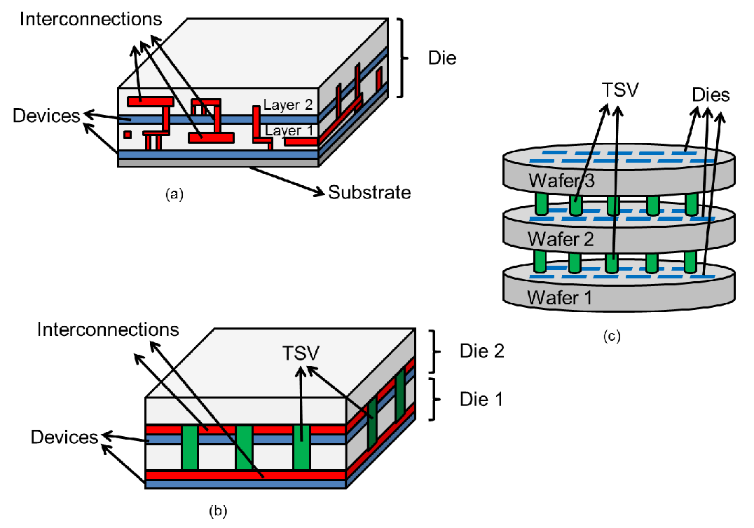
| Figure 1.5.: | Different implementations of a 3D IC: Monolithic device (a), Die-to-die integration (b), and Wafer-to-wafer integration (c). |
There are at least three different modes to implement 3D integration: Monolithic, die stacking, and wafer stacking [25]. The first relates to the construction of two or more device layers in one single wafer. The other two consist of piling up multiple die or wafers and a connection through the intermittent layers, as depicted in Fig. 1.5.
| Figure 1.5.: | Different implementations of a 3D IC: Monolithic device (a), Die-to-die integration (b), and Wafer-to-wafer integration (c). |
Naturally, every approach has a specific process to reach its final configuration. The maturity of the technology and the process involved in the fabrication will determine the mode to be adopted by industry. Monolithic devices are the farthest from commercial use and there are few reports from companies using this technology [26][27], while for die and wafer stacking there is a variety of publications from the industry and academy [28][29].
Die or wafers stacking presents similar challenges due to the nature of the concept. However, a very specific requirement for both methods is the communication between different stacked layers. A vertical interconnection is needed to go through the entire wafer in order to bind the devices in a 3D network. Those interconnections are known as Through Silicon Vias (TSV). The importance of the TSVs for the successful implementation of 3D integration is reflected in the great amount of literature available.