Next: 3.2 Secondary Generated Carriers Up: 3. Defect Creation Previous: 3. Defect Creation
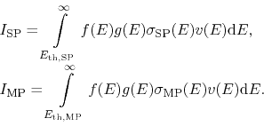
The carrier transport module described in Section 2.6 allows for a thorough evaluation of the carrier energy distribution function for a particular device architecture. The DF represents populations of "hot" and "colder" carriers and thus controls the interplay between the SP- and MP-mechanisms (see Section 1.4). Under real hot-carrier stress conditions both SP- and MP-mechanisms are present and their interplay is described by the shape of the distribution function reflecting the topological features of a particular device as well as the bias conditions. The DF enters the corresponding rates of the bond depassivation processes via the carrier acceleration integral
The integrand in (3.1) is obtained via the multiplication of the carrier flux with energies in the range [E; E + dE] by the probability to launch the reaction by a carrier at that energy. This flux is the product of the carrier distribution f(E), density-of-states g(E), and velocity v(E). Therefore, the SP- and MP-related AIs have the same functional structure and differ only in their parameters. Eth,SP/Eth,MP are (different) threshold energies of the SP/MP-processes and σSP/σMP the Keldysh-like reaction cross sections [99,32] - i.e. of the form
| (3.2) |
and the cross section for the MP-process has the same structure. The single-particle bond-breakage case refers to the excitation of the bonding electron to an antibonding state while the multivibrational mode excitation is linked to the excitation/decay of the phonon modes [99,32].
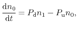
To find the interface state generation rate corresponding to the SP-process one should multiply the acceleration integral by the attempt rate νSP (which is the fitting parameter in the model), i.e. λSP = νSP ISP. Assuming the process follows first-order kinetics, the following dependence of the SP-related interface state density NSP on time is obtained
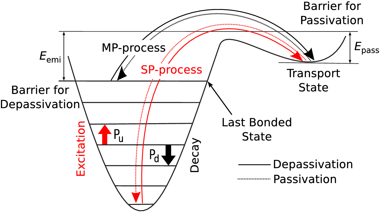
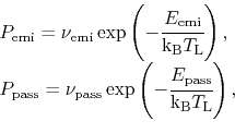
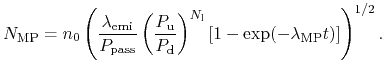
where n0 is the concentration of the virgin (passivated) Si-H bonds which can be broken. The situation with the MP-process is more complicated, because this process is linked to the excitation of the phonon modes by a cascade of the subsequent bombardments of the interface by carriers [30,31,99,32]. Note that the Si-H bond can relax from an excited state to a lower one, while the balance with a reciprocal process also must be considered. Therefore, the bond is treated as a truncated harmonic oscillator (Figure 3.1) characterized by the ladder of bonded levels. The last level is designated as Nl. The Si-H bond-breakage process is described by the system gradually climbing the ladder of energetic states, a process which is eventually terminated when hydrogen leaves the last bonded level for the transport state (Figure 3.1). The reaction rate is defined by the height of the barrier Eemi separating the last level and the transport state. Similarly, the passivation process is related to the hydrogen jumping into the opposite direction, determined by the barrier height Epass. The corresponding rates (Pemi,Ppass) are assumed to obey the Arrhenius law
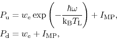
where (νemi,νpass) are attempt frequencies for the processes (fitting parameters), while TL is the lattice temperature. To obtain an expression for the phonon excitation and decay rates (Pu,Pd) (Figure 3.1) one can follow the formalism described in the papers by Hess et al. [99,32] (for a more details, see Section 1.4)
with we being the phonon frequency and ℏω the distance between the oscillator levels. The first two terms describe the population of the oscillator levels in the absence of the carrier acceleration while in the presence of the electron flux an additional term ISP/IMP enters the expression. The kinetics of the MP-process is determined by a system of rate equations (see e.g. [30])
 |
(3.6) |
 |
(3.7) |
 |
(3.8) |
As opposed to [30], in (3.8) all 4 terms are maintained (cf. with [30], Eq. 22): the first two are related to the oscillator excitation/deexcitation while the last two control the bond rupture and passivation
process. It is assumed that the MP-related interface state concentration is equal to the density of the mobile hydrogen which
is needed for the bond passivation. As a result, NMP enters (3.8) in the second degree.
To satisfy the dimensionality ![]() is used in (3.8).
is used in (3.8).
The model furthermore assumes that a steady-state between the individual energy levels is established rather quickly, much quicker than the hydrogen hopping step (depassivation/passivation). As a consequence, these reactions can be considered quasi-independently. Thus, first the last two terms in (3.8) are omitted and one considers the oscillator in equilibrium, i.e. one assumes that dni/dt = 0 for each i and recurrently finds that ni/n0 = (Pu/Pd)i (for the sake of simplicity it is also assumed that the oscillator is predominately in its ground state, i.e. n0 =∑i ni. Then it is possible to "switch on" hydrogen transitions and obtain the interface state evolution with time
It is worth emphasizing that in the case of weak stresses and/or short stress time, i.e. when λemit≪1, the expression (3.9) transforms to the root time dependence of NMP as reported in [30].
The two main Si-H vibrational modes are the stretching and bending modes [145,30], with their parameters listed in Table 1.1 [30]. It has been previously shown [63] that experimental data is better fitted by the bending mode and therefore for simulations one uses the parameters for this mode. The SP- and MP-processes lead to two types of traps which must have different distributions over energy in order to match with experimental data. Therefore, these mechanisms are considered independently, i.e. the total interface state density is calculated as the superposition of SP- and MP-related components weighted with corresponding probabilities
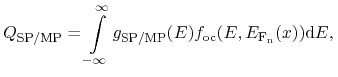
Only charged interface states contribute to the device performance degradation. Therefore, while modeling the transfer characteristic evolution during the hot-carrier stress one should consider effective charges stored in the interface states, not the total concentration Nit. These effective charges QSP and QMP, the total Qit is their sum) are defined as
where gSP (gMP) are the DOS for the SP(MP)-related traps and foc is the carrier distribution function obtained for device operation conditions. The coordinate-dependent position of the quasi-Fermi level of electrons is designated as EFn. Note that the functions gSP and gMP are coordinate dependent because of the normalization conditions, i.e.
 |
(3.12) |
The lateral coordinate also enters the DF for operation conditions because the quasi-Fermi level for carriers captured by traps is also position dependent. The model is thus calibrated in order to represent the degradation of the linear drain current Idlin over a wide range of stress and/or operation conditions by a proper determination of QSP and QMP.
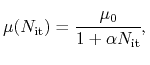
The carrier mobility in the device channel reduced after irradiation because of radiation-induced charges at the interface produces Coulomb scattering centers, which affect the motion of carriers in the channel. Therefore, the effective mobility, μ(Nit), which is related to the build-up of interface trapped charge, Nit, can be defined through the equation [165,166]
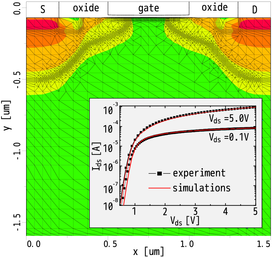
where μ0 is the mobility in absence of interface states, α is a proportionality coefficient.For the evaluation of the model a high voltage 5V n-type MOSFET fabricated on a standard 0.35um technology was used. The device cross-section/contour plot is schematically depicted in Figure 3.2. Since we are dealing with a long-channel device with a length of ~0.5um and a relatively high operating voltage of 5V, it is possible to estimate that the SP-process will dominate hot-carrier degradation.
|
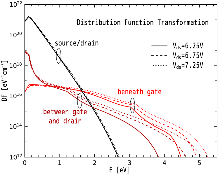
Figure 3.3a demonstrates the evolution of the carrier distribution function along the channel. One can see that near the source and drain the DF behaves like a heated Maxwellian, but has deep high energy-tails at the drain end of the gate. The carrier acceleration integral plotted vs. the coordinate x (Figure 3.3b) features its peak near the area with the most extended high-energy tails of the DF. Such a behavior proves that the hot-carrier induced damage is controlled by the carrier AI which is defined by the shape of the DF. The family of the effective Nit(x) profiles calculated over various operating conditions at a fixed stress time t of 10s is shown in Figure 3.3c and Figure 3.3d. One can see that MP-induced defects come into play only for Vgs ≥ 3.0V. This circumstance means that the SP- and MP-related states are differently distributed over energy with the latter shifted to higher energies. This result agrees with the concept by Hess et al. where the double-power law dependence of the degradation was explained by introducing two time slopes for defects created by different processes [24,40].
 (b)
(b)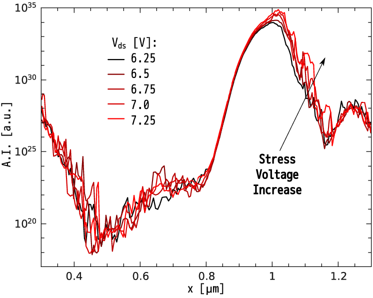
(c) 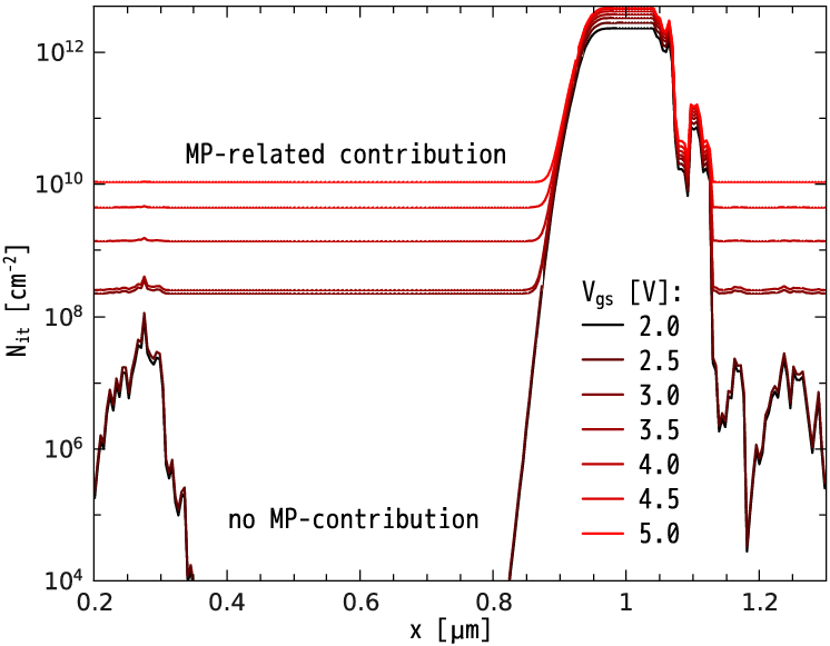 (d)
(d)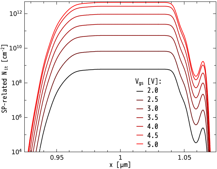
(e) 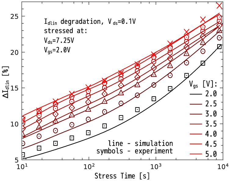 (f)
(f)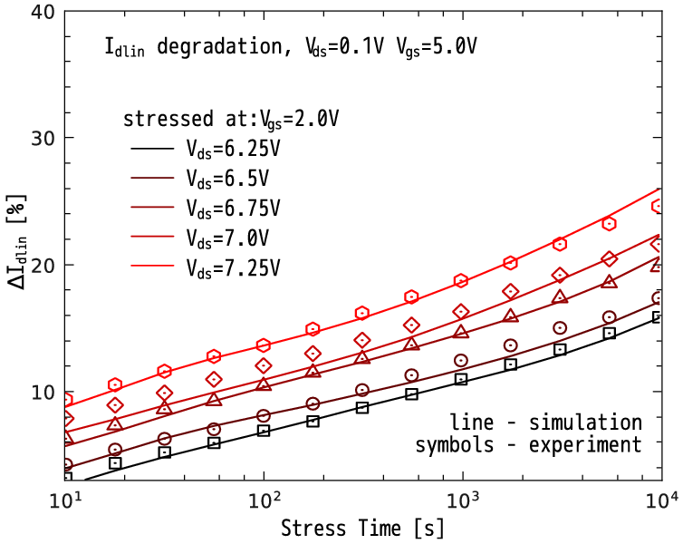
|
Figure 3.3d resolves the density of particles captured by the SP-traps in the region where the total trap concentration Nit is plotted for different Vgs. Since the main contribution to the total density Qit is provided by the MP-process one may compare the behavior of densities related to the different types of traps. For the SP-process the distance between the curves saturates, meaning that interface states of this type are almost fully occupied. In contrast, for the MP-process the increase of charge density continues.
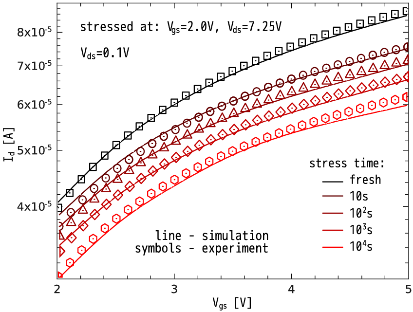
The model calibrated in the aforementioned manner allows for the Idlin degradation to be represented at various (Figure 3.3e) and for different stress conditions, i.e. different Vds (Figure 3.3f). There is no additional fitting parameter introduced into the model, which means that Nit effectively changes while switching from one stress condition to another. Finally, using this approach we are now able to represent the transfer characteristics of the degraded device at each time step, see Figure 3.4a.
 (b)
(b)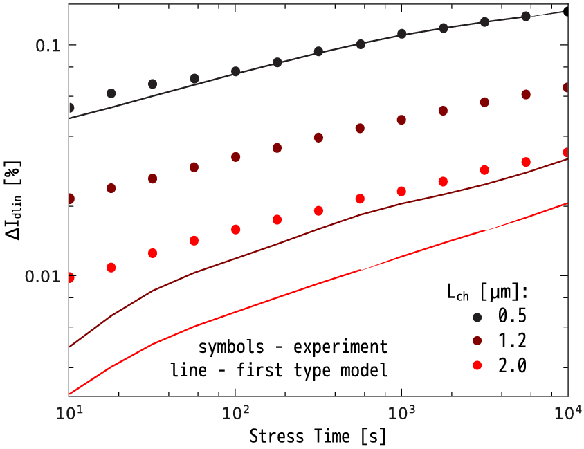
|
The approach described in this Section is able to successfully represent the linear drain current degradation for a wide range of stress/operating conditions in the case of a 5V n-MOSFETs with a channel length of Lch = 0.5um (Figure 3.2). Unfortunately, the model completely fails to capture Idlin degradation in MOSFET with different channel lengths with the same set of fitting parameters. In fact, for devices with Lch = 1.2 and 2.0um, the relative change of Idlin (i.e. the ratio between its absolute change and the value typical for a "fresh" device) predicted by the model is substantially less than that observed experimentally, see Figure 3.4b.