Next: 4.4 Analysis of the Threshold Voltage Turn-Around Effect Up: 4.3 Charge-Pumping Extraction Techniques Previous: 4.3.2 Comparison of Interface State Profiles Extracted with Different Capacitance Approaches
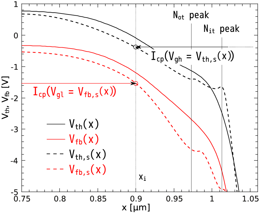
This extraction algorithm is based on the iterative correction scheme employing the equation system (4.13). The pre-stress CP edge is corrected for the additional charges associated with both Not(x) and Nit(x) generated due to the stress. For each position xi, the maximum possible range where the post-stress local threshold voltage can lie is found. By comparing the varying pulse-high and varying pulse-low measured CP currents under consideration for a chosen Vth(xi) valuefrom this range, Nit is separated from Not. Namely, for an assumed Vth(xi) using (4.11) Nit(xi) is calculated. Further, for a known value of the interface state density at xi, the local flatband voltage Vfb(xi) is found employing (4.12). The obtained results are Icp(Vgh = Vth(xi)) and Icp(Vgl = Vfb(xi)). Since the maximum value of the CP current Icp,max is the same for both varying high/low-level measurements (the effective channel length is the same), the following condition must be satisfied (see, Figure 4.15)
If (4.28) is not satisfied, the chosen Vth(xi) value is incorrect and it is necessary to repeat this procedure from the start. Otherwise, a solution is found and we can go to the next coordinate xi+1.
|
Here, it is assumed that Nit(x) follows the lateral electric field distribution along the channel. The main idea is that the damage profile can be modeled best as Gaussian. However, a Gaussian distribution is inconvenient for analytical modeling because the integral results in the error-function. Therefore, the authors suggest to model the Nit profile by an analytically integrable function with a similar shape
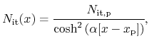
where Nit,p is the peak value of the damage, xp is the position of the peak along the channel and α is a parameter responsible for the spatial spread of the damage. This number of parameters is defined by the fitting procedure of experimental CP data. An implementation of (4.29) in (4.13) significantly simplifies the extraction process.
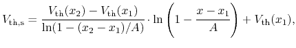
In this routine, it is supposed that the hot-carrier induced impact on Vth(x) for the damaged region near the drain side can be empirically represented as
while the undamaged region remains unchanged, i.e. Vth,s(x) = Vth(x). Here x1,2 are the boundaries of the damaged oxide region (defined by the evolution of the derivative of the charge-pumping curve with stress time) and A is the only unknown variable to be determined by the optimization technique. As in Mahapatra's approach, substituting of (4.30) in (4.13) results in a simplified defect profile characterization.
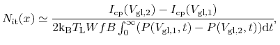
This technique stands out against the others because it requires only varying high-level measurements. At the same time, the suggested approach is original and worthy of attention. It is derived from the Shockley-Read-Hall theory which is used for the analytic charge-pumping current model. According to this model, Nit(x) is
where ![]() .
Here teme(temh) is the non-steady-state electron (hole) emission time measured from two low gate voltages (Vgl,1 and Vgl,2).
The fitting function P is obtained using device simulation and is equal to 1 at the center of the channel and rapidly decreases to 0 near the source/drain junction.
The oxide-trapped charge density is derived as Not(x) = ΔVcCox, where Vc is the difference of the voltage related to the half-maximum
value of the ΔIcp/f - Vgh curves.
.
Here teme(temh) is the non-steady-state electron (hole) emission time measured from two low gate voltages (Vgl,1 and Vgl,2).
The fitting function P is obtained using device simulation and is equal to 1 at the center of the channel and rapidly decreases to 0 near the source/drain junction.
The oxide-trapped charge density is derived as Not(x) = ΔVcCox, where Vc is the difference of the voltage related to the half-maximum
value of the ΔIcp/f - Vgh curves.
(a)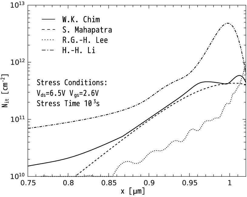 (b)
(b)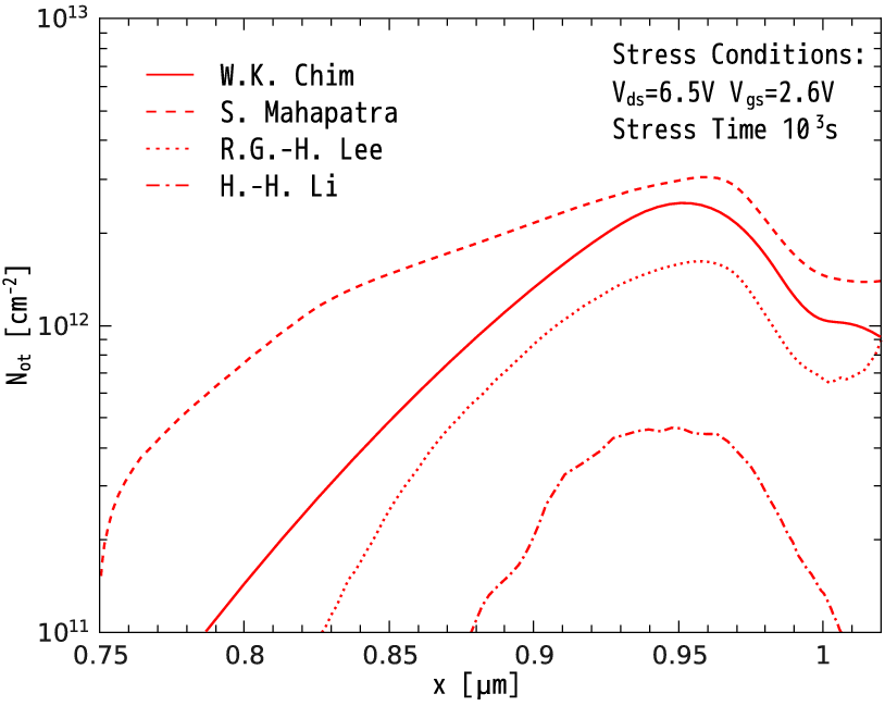
(c) 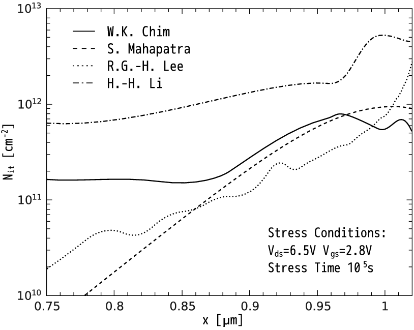 (d)
(d)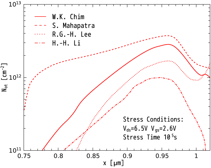
|
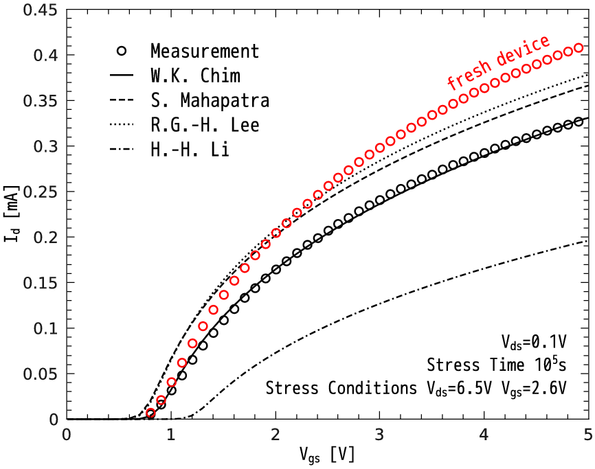
The profiles extracted for a stress time of 103s and 105s are depicted in Figure 4.16. The extracted Nit(x) and Not(x) dependences were subjected to further validation as input data of the device simulator MiniMOS-NT to model the transfer characteristics of the degraded device. A comparison of simulated and experimental curves checks the applicability of the considered techniques (see Figure 4.17).
One can see that the Id-Vds dependence evaluated with Li's model spuriously overestimates the damage as compared to other extraction schemes. This fact can be explained by the necessity to recalculate the P function after every iteration with an erroneously localized Not(x) profile as an input parameter. As mentioned above, the spatial distribution of the oxide traps is defined using the change of half maximum of the charge-pumping curve. Such a variation is a very insensitive parameter and, as a consequence, the technique for calculating Nit and Nit which is self-consistent, makes it questionable whether such additional efforts are justified [183].
At the same time, Mahapatra's approach predicts a transfer curve degradation close to the result obtained by Lee's method but not close enough to the experimental data. In literature one may find different criteria for evaluating the efficiency of interactions between the carriers and the bond, i.e. the maximum of the electric field, the carrier dynamic temperature, etc [29]. However, as proposed in Section 3.1, the Nit peak only corresponds to the maximum of the acceleration integral and is shifted away with respect to the maxima of other quantities. Consequently, for a proper HCD model it is not possible to use a simple analytical expression, such as (4.29) and (4.30). It is important to emphasize that the Nit(x) profiles extracted within Chim's technique features two peaks, see Figure 4.16a and Figure 4.16c. This finding is in good agreement with the results of the described HCD model, which shows that these peaks are related to the contributions induced by primary channel electrons and secondary generated holes (the latter is shifted towards the source) and correspond to the maxima of the electron and hole acceleration integrals (see Section 3.2). Moreover, in Section 3.1 one has already demonstrated that for long-channel devices the multiple-carrier process of Si-H bond-breakage leads to Nit homogeneously distributed over the interface, which is confirmed in Figure 4.16c (Nit plateau at the center of the gate).
|