Next: 4.5 HCD Caused Interface State Profile - Simulations vs. Experiment Up: 4. The Charge-Pumping Technique Previous: 4.3.3 Extraction Techniques Description
In this Section the turn-around effect of the threshold voltage shift during hot-carrier stress is investigated. Such a phenomenon is explained by the interplay between interface states and oxide traps, i.e. by the compensation of the rapidly created oxide charges by the more slowly created interface states. To prove this idea, a refined extraction scheme for the defect distribution from charge-pumping measurements has been employed. The obtained results are in good agreement with the findings of the proposed physics-based model of hot-carrier degradation (see Section 3.2). The approach considers not only damage produced by channel electrons but also by secondary generated channel holes. Although the contribution of the holes to the total defect creation is smaller compared to that of electrons, their impact on the threshold voltage shift is comparable with the electronic one. The reason behind this trend is that hole-induced traps are shifted towards the source, thereby more severely affecting the device behavior.
It is commonly accepted that processes related to trapping/detrapping in the oxide bulk play a crucial role in the bias temperature instability (BTI) [186,187]. Since BTI and hot-carrier degradation are believed to have a similar microscopic origin, one may expect that bulk oxide traps with the density Not should also contribute to HCD. At the same time, Not dominates the recoverable component of BTI [138], suggesting that HCD should also recover considerably. However, in n-MOSFETs hot-carrier degradation demonstrates a rather small recovery over a wide range of temperatures [41,29]. The situation is made even more complicated because of turn-around effects sometimes observed during hot-carrier stresses [109,173]. These turn-around effects are related to the partial compensation of the charge stored in the oxide traps by interface state trapping characterized by the density Nit [173,29]. It is worth emphasized that a systematic study considering the evolution of the lateral defect profiles with stress time has not been carried out. The main scope of this part of the work is to analyze the turn-around of the Vth shift observed during HC stress. This strategy is supported by charge-pumping data and is linked to the developed HCD model. The model considers not only channel electrons but also secondary holes generated by impact ionization caused by the injection of hot electrons. These holes are then accelerated by the electric field towards the source, thereby creating interface states shifted with respect to the electron-induced ones. As a result, the Nit fraction induced by holes should be much less than their relative contribution to the linear drain current change (see Section 3.2).
For an investigation of the turn-around effect a 5V n-type MOSFET fabricated in a standard 0.35um CMOS process (depicted in Figure 3.2) is employed. The device channel length is 0.5um. The device was stressed at three combinations of drain and gate voltages: {Vds,Vgs} = {6.5,2.6}, {6.75,2.0} and {6.25,2.0}V and a temperature of T = 40oC. Such a temperature regime was used because trapping/detrapping in the oxide bulk is triggered by non-elastic trap-assisted tunneling which is accelerated at higher temperatures [188,189]. In the inset of Figure 4.18 the shift of the threshold voltage Vth vs. the stress time is depicted. One can see that the turn-around effect of the Vth shift [173] is less pronounced at room temperature. These turn-around effects are related to a partial compensation of the charge stored in the oxide traps by interface state trapping [29]. In this context, the chuck temperature was set to 40oC to accelerate the degradation processes.
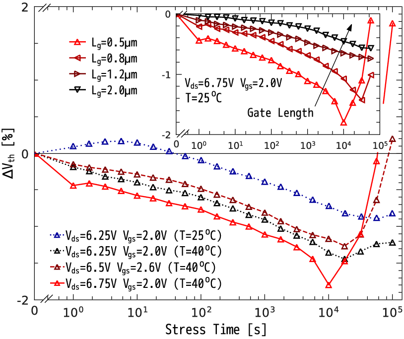 |
Based on the analysis of Section 4.3, stress voltages close to the WCC were intentionally chosen in order to maximize the contribution of all degradation effects. The threshold voltage was monitored up to 105s. Figure 4.18 demonstrates that Vth first decreases due to hole trapping in the oxide bulk while after 103s Vth increases due to the trapping of electrons by interface traps. To check these speculations, the CP technique with varying amplitude of the gate pulse [177,66] has been employed to investigate the Nit(x) and Not(x) distributions. A standard experimental scheme is used, where the gate of the transistor is connected to a pulse generator and a small constant reverse bias is applied to the source and drain. The measured current is the substrate current and a gate pulse frequency is 25kHz. A measurement setup is used with Vgl = -5V Vgh is increased from -4 to 2V (varying high level technique) and Vgh = 3V with decreasing Vgl from 2 to -5V (varying base level technique) in 0.02V increments.
Furthermore, to extract the evolution of Nit(x) and Not(x) profiles with the stress time, the analytical Cox(x) distribution (4.23) incorporated into the scheme of Chim's et al. extraction technique [177], based on system (4.13) is employed. The extracted Nit(x) profile features two peaks, see Figure 4.19. This finding is in good agreement with the results of the developed HCD model which shows that these peaks are related to the contributions induced by primary channel electrons ans secondary generated holes (note that the latter one is shifted towards the source). In Section 3.1 and Section 3.2 it is demonstrated that in long-channel devices the multiple-carrier process of Si-H bond-breakage leads to Nit homogeneously distributed over x (see Figure 4.19).
(a)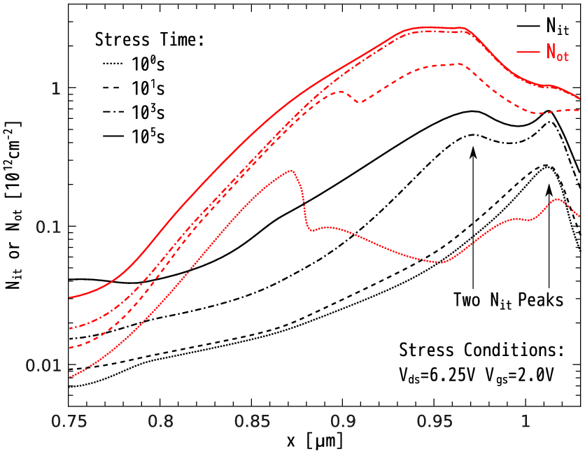 (b)
(b)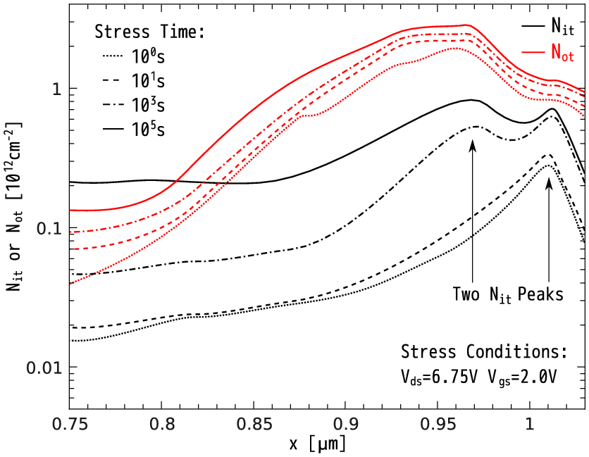
|
At the same time, this is the component which gives the main contribution to ΔVth because the device is most sensitive to Nit created closer to the channel middle (and in this device area the SP-related contribution is negligible). Hence, notwithstanding the fact that the maximum value of Not is higher than the initial Nit peak value (Figure 4.19), Nit starts to prevail over Not at longer times (⩾104s in this particular case). This is because at these times only the peak Not value is higher than the Nit maximum while within the device center (which defines the Vth behavior) Nit is higher. The strong localization of the Nit SP-component near the drain edge of the gate and, as a consequence, the secondary influence on ΔVth can be confirmed by the saturation of Vth and a turn-around effect. This trend is depicted in Figure 4.18, inset for four MOSFETs of the same architecture with different gate lengths.
One may conclude that the hole contribution is considerably shifted towards the source. The single-electron component generates traps situated outside of the channel which explains why the hole-induced traps have a stronger relative impact on the threshold voltage turn-around effect. The contribution of channel holes to the total defect concentration is much less than the corresponding fraction of Vth change. This trend becomes more pronounced for longer devices (Figure 4.18, inset), see also Section 3.2. Another tendency confirming these considerations is that the ΔVth turn-around effect is less pronounced at room temperature (Figure 4.18 for the stress regime with Vds = 6.25V and Vgs = 2.0V). This is because trapping/detrapping in the oxide bulk is triggered by non-elastic trap-assisted tunneling which is accelerated at higher temperatures [188].
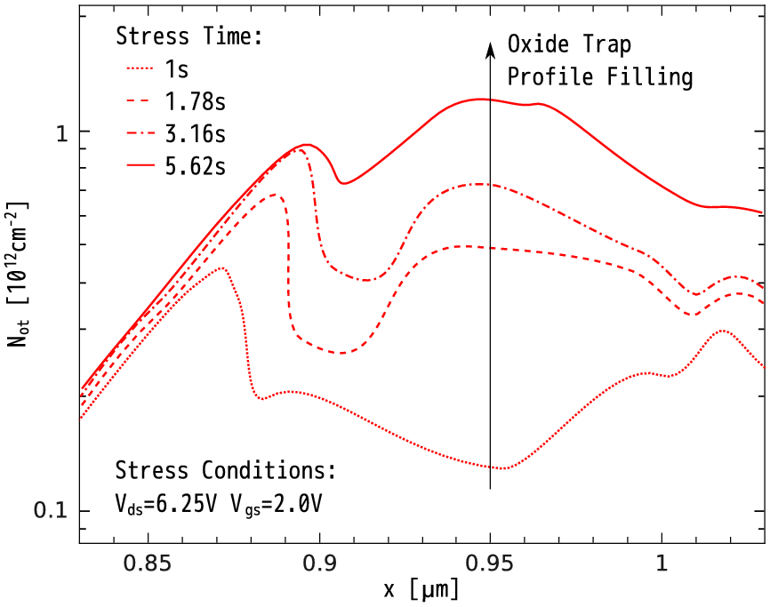
In Figure 4.20 the Not(x) profiles are resolved for short stress times. Initially, two peaks are differently positioned in space while after ~5s they unite into a single common hump. It is worth emphasizing that the position of the Nit(x) and Not(x) peaks does not change with time (Figure 4.19). This is in good agreement with the model predictions where the position of the carrier acceleration integral maximum coincides only with the Not(x) peak position.
|