To identify the critical doping parameters and, therefore, the relevant doping
regions, a sensitivity analysis is carried out. This procedure is similar to
a gradient calculation during optimization. Each optimization parameter is
slightly increased from its optimal value and the changes in the drive and
leakage currents are used to calculate the sensitivity values. For example,
the relative sensitivity of the drive current
![]() on the
optimization parameter
on the
optimization parameter
![]() is calculated by
is calculated by
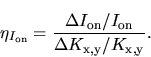 |
(4.3) |
The sensitivities can be visualized on the optimization grid within the inverted-T region. The results are shown in Fig. 4.6 for Device Generation A and in Fig. 4.7 for Device Generation B.
![\resizebox{0.71\textwidth }{!}{
\psfrag{x [um]} [ct][cb]{$x$\ ($\mu$m)}
\psfrag{...
...cs[height=0.71\textwidth ,angle=90]{../figures/3D-SA-ion-0.25-drivecurrent.eps}}](img116.gif)
![\resizebox{0.71\textwidth }{!}{
\psfrag{x [um]} [ct][cb]{$x$\ ($\mu$m)}
\psfrag{...
...s[height=0.71\textwidth ,angle=90]{../figures/3D-SA-ioff-0.25-drivecurrent.eps}}](img117.gif)
|
![\resizebox{0.71\textwidth }{!}{
\psfrag{x [um]} [ct][cb]{$x$\ ($\mu$m)}
\psfrag{...
...cs[height=0.71\textwidth ,angle=90]{../figures/3D-SA-ion-0.10-drivecurrent.eps}}](img118.gif)
![\resizebox{0.71\textwidth }{!}{
\psfrag{x [um]} [ct][cb]{$x$\ ($\mu$m)}
\psfrag{...
...s[height=0.71\textwidth ,angle=90]{../figures/3D-SA-ioff-0.10-drivecurrent.eps}}](img119.gif)
|
One important region is pointed out located in the channel region, slightly beneath the silicon surface, close to the source well. Looking at the optimization results in Fig. 4.4 and Fig. 4.5 it can be seen that at this position the doping has a local maximum. In Chapter 5 it will be shown that this doping peak sets the threshold voltage of the device and reduces the effective channel length increasing the drive performance of the transistor.
The sensitivities of the drive and leakage currents look pretty much alike for
both device generations. This is because a change in the acceptor doping
affects both the drive and leakage current in the same way. Anyway, the
highly doped regions underneath the source and drain wells in
Fig. 4.4 and Fig. 4.5 were expected to influence the
leakage current in a stronger way than they influence the drive current
because the background doping is low (10![]() cm
cm![]() )
and the doping
regions under source and drain work as a kind of shield against deep
punchthrough. But as the doping in these regions is quite high which means
that the shield is stronger than necessary to prevent punchthrough, a small
change in the doping hardly affects the leakage current. The optimization
delivered this high doping under source and drain because there was no
constraint that would work against it, for example, if the drain-bulk leakage
due to carrier tunneling across the abrupt junction was considered. This
effect is much stronger for a higher doping under the drain well.
)
and the doping
regions under source and drain work as a kind of shield against deep
punchthrough. But as the doping in these regions is quite high which means
that the shield is stronger than necessary to prevent punchthrough, a small
change in the doping hardly affects the leakage current. The optimization
delivered this high doping under source and drain because there was no
constraint that would work against it, for example, if the drain-bulk leakage
due to carrier tunneling across the abrupt junction was considered. This
effect is much stronger for a higher doping under the drain well.