The semiconductor equations discussed above show the basic relations between carrier distribution and the electrostatic potential. Two parameters, the mobility and the recombination rate were introduced, which require appropriate modeling. The physical phenomena which are crucial for modeling of these parameters will be discussed in the following.
The derivation of the mobility originates from carrier relaxation times. The mobility is influenced by the lattice and its thermal vibrations, impurity atoms, surfaces and interfaces, interface charges and traps, the carriers themselves, the energy of the carriers, and other effects like lattice defects. Mobility models are used to make an estimation considering these effects and make simulations in continuous systems possible. Since exact derivations are too complex or just do not exist, empirical approaches are often used. Some of the commonly used approaches will be presented here.
A common method for modeling the mobility is the hierarchically encapsulation
of the physical mechanisms. In this approach, the most fundamental mechanism is
considered to be the lattice scattering dependence (
![]() )
followed by the ionized impurity dependence (
)
followed by the ionized impurity dependence (
![]() ). Especially in
MOS devices, a surface correction (
). Especially in
MOS devices, a surface correction (
![]() ) is of special
importance. These three contributions classify the low-field mobility
models. Modeling of high-field effects is introduced with a field dependence
model (
) is of special
importance. These three contributions classify the low-field mobility
models. Modeling of high-field effects is introduced with a field dependence
model (
![]() ). These contributions can be combined like in the
MINIMOS mobility model [138], for example, which looks like
). These contributions can be combined like in the
MINIMOS mobility model [138], for example, which looks like
Effects like negative bias temperature instability [143] or hot carrier degradation (see Chapter 6) generate interface traps leading to interface charges. Modeling of their influence on the mobility is of special interest in reliability modeling [144]. A mobility reduction due to oxide charges in inversion layers has been proposed by Sun et al. [145] as
The carrier mobility also depends on the carrier energy distribution. However, in the drift-diffusion model the electric field is usually employed. Simulation tools commonly differ between low- and high-field mobility and let the user select the models independently. The high-field mobility modeling approaches are often accomplished using the model presented by Caughey and Thomas [147]. A slightly different version, suggested by Jaggi [148,149], is used in the MINIMOS mobility model,
![\includegraphics[width=0.47\textwidth]{figures/MM6LIS.eps}](img206.png)
![\includegraphics[width=0.47\textwidth]{figures/MM6LISF.eps}](img207.png)
|
To illustrate the impact of mobility models a comparison of simulation results
with constant mobility, a low-field mobility model, and a high-field mobility
model are shown in Fig. 4.4. Comparing the constant
mobility and the low-field mobility model, one can see that the shape changes
only slightly, but the total current is reduced significantly for the low-field
mobility model (note the multiplication factors in the legend). This is caused
by the reduction of the mobility, especially near the surface, which can be
clearly seen in Fig. 4.3. The transconductance is only
slightly influenced, whereas for the high-field mobility model, a strong
reduction can be observed. Hence, for the ![]() V curve, it can be seen
clearly that the current initially increases steeply with the drain voltage,
but immediately flattens, since the mobility reduction becomes effective. The
effective mobility distribution at
V curve, it can be seen
clearly that the current initially increases steeply with the drain voltage,
but immediately flattens, since the mobility reduction becomes effective. The
effective mobility distribution at
![]() V can be seen in
Fig. 4.3.
V can be seen in
Fig. 4.3.
![\includegraphics[width=0.6\textwidth]{figures/DD_mobcomparison.eps}](img210.png) |
Carrier mobility modeling has been investigated since the beginning of semiconductor engineering, and there are still new models published [150]. However, all approaches in the drift-diffusion model which incorporate the influence of carriers that are not in thermal equilibrium basically rely on the electric field. Changes in the electric field therefore directly change the calculated mobility (see Fig. 4.5), whereas the distribution function and therefore the carrier temperature do not change immediately. Mobility models in higher-order transport models can use more information from the distribution function. In energy-transport, for example, the carrier temperature can be used as a parameter. As a consequence effects like the velocity overshoot can be described.
![\includegraphics[width=1.0\textwidth]{figures_book/my_vo.eps}](img211.png)
|
The recombination rate ![]() was formally introduced in the drift-diffusion
equations (4.5) and (4.6) by splitting the continuity
equation into two individual parts for electrons and holes. From a physical
point of view this term includes the generation and the recombination of
electron-hole pairs. In thermal equilibrium carrier generation and
recombination are balanced and the carrier concentrations are given by their
equilibrium values
was formally introduced in the drift-diffusion
equations (4.5) and (4.6) by splitting the continuity
equation into two individual parts for electrons and holes. From a physical
point of view this term includes the generation and the recombination of
electron-hole pairs. In thermal equilibrium carrier generation and
recombination are balanced and the carrier concentrations are given by their
equilibrium values ![]() and
and ![]() (
(
![]() ). The net recombination
rate therefore vanishes. An excess number of carriers leads to an increased
recombination, a low carrier concentration leads to an increased
generation. The generation and recombination processes contributing to the
total effective net generation rate are based on different physical effects
which are modeled independently of each other. The separately evaluated models
add up to the total net recombination rate. The resulting rate is used to
complete the continuity equations (4.5) and (4.6).
). The net recombination
rate therefore vanishes. An excess number of carriers leads to an increased
recombination, a low carrier concentration leads to an increased
generation. The generation and recombination processes contributing to the
total effective net generation rate are based on different physical effects
which are modeled independently of each other. The separately evaluated models
add up to the total net recombination rate. The resulting rate is used to
complete the continuity equations (4.5) and (4.6).
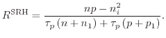
One important generation/recombination process is the well-known Shockley-Read-Hall (SRH) mechanism [152,153] which describes a two-step phonon transition. One trap level which is energetically located within the band-gap is utilized. Four partial processes can be separated: the capture and the emission of both, electrons and holes, on the trap level. Balance equations can be formulated for the trap occupancy function. In the stationary case the rates for electrons and holes are equal. The trap occupancy function can then be eliminated and the SRH generation rate results in
In MOS devices SRH generation especially influences the bulk current. In n-channel devices, for example, holes generated at the pn-junction are attracted by the low bulk potential leading to the bulk current. The influence can be easily observed in device simulation since models can be switched on or off allowing to deactivate SRH. Fig. 4.6(a) shows the hole current flow and the SRH generation rate in the sample device and in Fig. 4.6(b) the current components on the bulk contact are compared with and without SRH enabled.
![\includegraphics[width=0.48\textwidth]{figures/SRH.eps}](img220.png)
![\includegraphics[width=0.49\textwidth]{figures/SRH_bulk.eps}](img221.png)
|
The SRH model is not restricted to the description of capture and emission of carriers in the bulk, it can also be extended to determine the occupancy of interface traps [154]. Like most interface related mechanisms this is especially relevant for MOS devices. Simulations of charge pumping (CP) measurements [155], which are used to determine interface trap distributions, require appropriate modeling of trapping and de-trapping effects of carriers in interface traps. In a CP-simulation the measurement procedure is replicated, by performing a transient simulation for each gate pulse level (Fig. 4.7(a)).
![\includegraphics[height=70mm]{figures/CP_trans.eps}](img222.png)
![\includegraphics[height=70mm]{figures/CP_I.eps}](img223.png)
|
In contrast to the stationary SRH formulation shown in (4.15), time dependent simulations require to capture the transient behavior of the occupancy function [156]. The final charge pumping curve can be constructed by extracting the mean bulk current of the simulations for every single gate pulse (Fig. 4.7(b)).
In addition to the two-particle SRH mechanism there are other important generation mechanisms to mention: the Auger and the impact-ionization process, both of which are three-particle processes. The impact-ionization process, a very important mechanism when considering hot-carrier processes, is discussed in detail in Chapter 5. The Auger generation is a pure generation process. The energy required for carrier generation is delivered by a third higher-energetic electron or hole. In the Auger process, additionally the excess energy which is available after a recombination process is transferred to a third particle electron or hole. Modeling of this process can be achieved by defining rates for each partial process. In the stationary case the rate evaluates to [11]
| (4.16) |
There are various other generation and recombination mechanisms which have not been mentioned here. Among them are, just to mention a few, the direct recombination which is crucial for direct bandgap semiconductors, the direct [159] and trap assisted [160] band-to-band tunneling in high field regions, and optical generation [11].
Many physical properties of semiconductor devices strongly depend on the lattice temperature. Especially in high-voltage and power devices, the self-heating of the device is of special importance and the temperature distribution within a device is needed to estimate the device behavior at operating conditions. Regions of special interest are associated to high-current densities. In MOSFETs, these regions are commonly at the drain end of the channel, in the drain extensions and drift zones, and at corners [161].
For the definition of a reference temperature and for the dissipation of the generated heat, the simulation domain must be connected to one or more external reference temperatures or heat sinks. This connection is modeled in terms of thermal contacts, which have assigned fixed temperatures and are connected to the simulation domain via thermal resistances. It is also important to consider that the heat flow in a semiconductor device extends to areas that are electrically less important. Hence, the simulation domain usually has to be extended in comparison to iso-thermal simulations [162]. At the simulation domain boundaries representing symmetries in the device, Dirichlet conditions are used. For a proper modeling of corner effects, a three-dimensional simulation has to be used [163,164].
The lattice temperature distribution
![]() is modeled using the heat conduction
equation [127]
is modeled using the heat conduction
equation [127]
 |
(4.17) |
Different approaches of modeling the heat generation rate ![]() have been
proposed. The most simple approach considers only the Joule heat
have been
proposed. The most simple approach considers only the Joule heat
![]() [165]. A more accurate model according to Adler [166]
describes the generated heat using
[165]. A more accurate model according to Adler [166]
describes the generated heat using
Transient simulations including thermal modeling were performed using the
sample device. The lower bulk contact is linked with a thermal resistance to
the ambient temperature of
![]() In this simulation, the drain
voltage is raised linearly from
In this simulation, the drain
voltage is raised linearly from
![]() to
to
![]() using two
different slopes. The temperature distributions at the end of the two voltage
ramps are depicted in Fig. 4.8. At the end of the
using two
different slopes. The temperature distributions at the end of the two voltage
ramps are depicted in Fig. 4.8. At the end of the
![]() slope a rapid increase of the temperature near the birds beak
can be observed.
slope a rapid increase of the temperature near the birds beak
can be observed.
|
In addition to the physical mechanisms addressed so far, there are many other relevant modeling issues for semiconductor devices. For most of them, well established approaches are available in TCAD device simulation environments. The simulation tools typically incorporate models for the bandgap energy and for bandgap narrowing [167]. At low temperatures, incomplete ionization becomes important [168]. Also, semiconductor-metal contacts require appropriate treatment. The most common contact models are the well-known ohmic contact model, where charge neutrality and equilibrium are assumed at the electrodes [11], and the Schottky contact model [32].
Especially in highly down-scaled MOS devices, tunneling and quantum effects have to be considered. For direct tunneling typically the Tsu-Esaki [169] or the Fowler-Nordheim [170] models are used. Herrmann and Schenk [171] proposed models for trap assisted tunneling, which has also been extended to multi-trap assisted tunneling models [172], especially interesting for highly degraded devices.
The inclusion of quantum confinement effects becomes especially important in modern devices [173] like silicon-on-insulator (SOI) structures, double-gate or FinFET devices. One modeling proposal is the modified local density approach [174] which is used in the model of Hänsch [175]. Here, a local correction of the effective density of states near the gate oxide is used to contribute to the quantum effects. An empirical correction approach has been presented by Van Dort et al. [176] which models the quantum confinement by increasing the band-gap near the interface.
![\includegraphics[width=0.47\textwidth]{figures/temperature_70ns.eps}](img239.png)
![\includegraphics[width=0.47\textwidth]{figures/temperature_700ns.eps}](img241.png)