The carrier energy distribution function gives important information on the state of carriers in semiconductor devices. The detailed knowledge of the distribution allows an accurate estimation of the carrier mobility, the impact-ionization rates, and of other carrier energy dependent issues. As already pointed out earlier in this chapter, the carrier distribution function is described by the semi-classical BTE [123,15].
The average carrier energy, commonly expressed through the carrier temperature, is available in energy-transport/hydrodynamic transport models [131,132]. The carrier temperature is solved as an independent quantity, where the heated Maxwellian distribution function is used for the formulation of the closure relation.
In the drift-diffusion framework the distribution function is assumed to be a cold
Maxwellian distribution and the carriers are per definition in thermal
equilibrium, meaning that the carrier temperature (![]() ) equals the lattice
temperature (
) equals the lattice
temperature (
![]() ). There is no information on the distribution function
available. However, to estimate the carrier temperature
). There is no information on the distribution function
available. However, to estimate the carrier temperature ![]() the local
energy balance equation in the stationary, homogenous case in bulk is often
used. With
the local
energy balance equation in the stationary, homogenous case in bulk is often
used. With ![]() for electrons and
for electrons and ![]() for holes, the estimation reads
[15,177]
for holes, the estimation reads
[15,177]
| (4.20) |
|
It is possible to perform further simplifications on
(4.19): For moderate fields, the mobility can be assumed
as constant, which leads to
![]() For increasing fields the
carrier velocity approaches the saturation velocity
For increasing fields the
carrier velocity approaches the saturation velocity
![]() and the
mobility can be estimated as
and the
mobility can be estimated as
 |
(4.21) |
In two- or three-dimensional simulations, one has to consider that the
perpendicular component of the electric field on the current flow has no impact
on the carrier energy. The electric field in (4.19) is
therefore often replaced by the electric field projected in the direction of
the current density,
![]() In
Fig. 4.10 this method is applied on a simple planar
MOS transistor and compared to results from a hydrodynamic simulation.
In
Fig. 4.10 this method is applied on a simple planar
MOS transistor and compared to results from a hydrodynamic simulation.
|
A more detailed comparison with Monte Carlo data along the channel of an
![]() µm n-MOS device is shown in Fig. 4.11.
µm n-MOS device is shown in Fig. 4.11.
![\includegraphics[width=0.6\textwidth, clip]{figures/carriertemp_device.eps}](img274.png) |
In Fig. 4.9 one can see, that the carrier temperature
already doubles at electric fields which are in the order of
![]() kV/cm. Considering that fields in devices can reach up to
kV/cm. Considering that fields in devices can reach up to
![]() MV/cm, it is clear that the deviation from the assumption of equal
carrier and lattice temperature has to be taken into account for hot-carrier
reliability considerations as will be discussed in Chapter 6.
MV/cm, it is clear that the deviation from the assumption of equal
carrier and lattice temperature has to be taken into account for hot-carrier
reliability considerations as will be discussed in Chapter 6.
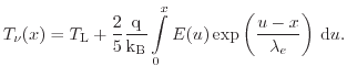
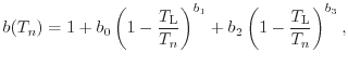
Sofar only the local electric field was used to model the carrier temperature. However, carriers do not gain or loose the energy as fast as the electric field changes. This non-local behavior is especially relevant for rapidly changing electric fields (see Fig. 4.5 f:dm.velocity_overshoot). The electric field is the only quantity in drift-diffusion simulations that can be used to estimate the carrier temperature. Approaches have been suggested to estimate this non-local behavior using the electric field. In the approach by Slotboom et al. [179], the temperature along a one-dimensional path is derived from a simplified, stationary one-dimensional energy balance equation, which reads
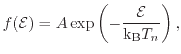
The real distribution function in a MOS transistor in a down-scaled technology node under operation conditions varies strongly along the channel and commonly differs from the Maxwellian shape. Targeting on hot-carrier reliability considerations, especially the high-energy tail which describes the hot-carrier population is of major importance. This section examines only the electron distributions and the approximations are based on the electron temperature, although the shape of the distribution function can vary strongly for the same temperatures (compare Fig. 4.2 f:dm.nonlocal). It is also important to consider that a change in the hot-electron population of an order of a magnitude usually hardly changes the mean temperature of the total electron population but strongly influences hot-carrier effects like the impact-ionization rate (see Chapter 6). The hot-electron tail is not captured at all in the cold Maxwellian distribution,
 |
(4.24) |
 |
(4.25) |
|
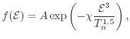
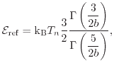
A better approach to represent the high energy part of the distribution function was proposed by Cassi and Ricò as [180]
Another approach was given by Grasser et al. [182] who proposed to use the electron distribution function
 |
(4.30) |
A special variation of the last representation has been used in the attempt to
simulate hot-carrier degradation in the drift-diffusion framework as described in
Section 6.4.1. Here
the exponent ![]() in (4.28) has been empirically set
to
in (4.28) has been empirically set
to ![]() and
and
![]() has still been
evaluated using (4.29). As described in the referred
section, this approximation delivers in the given sample the best agreement to
the Monte Carlo results.
has still been
evaluated using (4.29). As described in the referred
section, this approximation delivers in the given sample the best agreement to
the Monte Carlo results.
Comparing the different approximations, one has to distinguish the specific
conditions along the MOS channel area. At the position ![]() µm
(Fig. 4.12(a)) the carriers have not been accelerated yet
and are in thermodynamic equilibrium. As can be seen in
Fig. 4.11, the electron temperature of the drift-diffusion
solution matches the lattice temperature at
µm
(Fig. 4.12(a)) the carriers have not been accelerated yet
and are in thermodynamic equilibrium. As can be seen in
Fig. 4.11, the electron temperature of the drift-diffusion
solution matches the lattice temperature at
![]() Only the
distribution function model by Cassi cannot reproduce the result due to the
fixed parameters in (4.26). At
Only the
distribution function model by Cassi cannot reproduce the result due to the
fixed parameters in (4.26). At ![]() µm
(Fig. 4.12(b)) and
µm
(Fig. 4.12(b)) and ![]() µm
(Fig. 4.12(c)) it is obvious, that the cold Maxwellian
distribution does not reproduce the electron distribution at all and the heated
Maxwellian distribution only approximates the Monte Carlo results at low
energies. Any conclusion on high energy processes would clearly lead to
overestimations. The approaches by Cassi and Grasser at least catch the trend
of the Monte Carlo results. In this example, the Grasser approach also captures the
trend of the growing high energy tail at
µm
(Fig. 4.12(c)) it is obvious, that the cold Maxwellian
distribution does not reproduce the electron distribution at all and the heated
Maxwellian distribution only approximates the Monte Carlo results at low
energies. Any conclusion on high energy processes would clearly lead to
overestimations. The approaches by Cassi and Grasser at least catch the trend
of the Monte Carlo results. In this example, the Grasser approach also captures the
trend of the growing high energy tail at ![]() µm. This is true for a
constant and a calculated
µm. This is true for a
constant and a calculated ![]() value. Finally, at the position
value. Finally, at the position ![]() µm
(Fig. 4.12(d)) the shortcoming of the drift-diffusion equations
becomes very clear. The field and therefore the electron temperature has
already dropped, but there exists a high energy population of carriers, which
still can strongly influence high energy processes. The distribution by Cassi
does not catch this tendency, the other distributions match the cold
Maxwellian. This last condition, which is already in the highly doped drain
area of this transistor, cannot be described at all using the drift-diffusion framework.
µm
(Fig. 4.12(d)) the shortcoming of the drift-diffusion equations
becomes very clear. The field and therefore the electron temperature has
already dropped, but there exists a high energy population of carriers, which
still can strongly influence high energy processes. The distribution by Cassi
does not catch this tendency, the other distributions match the cold
Maxwellian. This last condition, which is already in the highly doped drain
area of this transistor, cannot be described at all using the drift-diffusion framework.
All estimates of the distribution function which are solely based on the electric field and/or the mean carrier temperature, can only lead to good results in special applications. One approach to overcome this is to handle two different carrier populations, one for hot and one for cold carriers [184]. For this, transport equations have to be solved for both populations and rate equations for carrier interchange between both populations.
The probably best macroscopic approach to capture the high-energy tail
correctly all over the device is to apply higher order moment transport
equations with at least six moments [134] of the BTE. In the six moments
model additionally to the mean carrier temperatures ![]() the kurtosis
the kurtosis
![]() is available which quantifies the deviation of the distribution
function from the Maxwellian shape. Grasser et al. [134] made the
following proposal, similar to the one from Sonoda et al. [185],
is available which quantifies the deviation of the distribution
function from the Maxwellian shape. Grasser et al. [134] made the
following proposal, similar to the one from Sonoda et al. [185],
![\includegraphics[width=0.6\textwidth]{figures/df_sm}](img319.png) |
![\includegraphics[width=0.51\textwidth]{figures/carriertempfit_n_1e16.eps}](img258.png)
![\includegraphics[width=0.51\textwidth]{figures/carriertempfit_n_1e20.eps}](img260.png)
![\includegraphics[width=0.51\textwidth]{figures/carriertempfit_p_1e16.eps}](img262.png)
![\includegraphics[width=0.51\textwidth]{figures/carriertempfit_p_1e20.eps}](img264.png)
![\includegraphics[width=0.49\textwidth, clip]{figures/ctm_dd_}](img271.png)
![\includegraphics[width=0.49\textwidth, clip]{figures/ctm_hd_}](img272.png)
![\includegraphics[width=0.51\textwidth]{figures/dist_compare_600.eps}](img283.png)
![\includegraphics[width=0.51\textwidth]{figures/dist_compare_900.eps}](img285.png)
![\includegraphics[width=0.51\textwidth]{figures/dist_compare_1000.eps}](img287.png)
![\includegraphics[width=0.51\textwidth]{figures/dist_compare_1100.eps}](img289.png)
![$\displaystyle f(\ensuremath{\mathcal{E}}) = A \left[ \exp \left( - \frac{\chi_a...
...p \left(- \frac{\chi_b \ensuremath{\mathcal{E}}^3}{T^{1.5}_n} \right) \right] .$](img293.png)
![$\displaystyle f(\ensuremath{\mathcal{E}}) = A \exp \left[ - \left( \frac{\ensuremath{\mathcal{E}}}{\ensuremath{\mathcal{E}}_\mathrm{ref}} \right) ^b \right] .$](img298.png)
![$\displaystyle f(\ensuremath{\mathcal{E}}) = A \left\{ \exp \left[ - \left( \fra...
...frac{\ensuremath{\mathcal{E}}}{\ensuremath{\mathrm{k_B}}T_2} \right] \right\} ,$](img314.png)