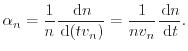
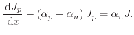
Impact-ionization is a three-particle generation process. Carriers that gain high energies while traveling through high field regions undergo scattering events with bonded electrons in the valence band. The excess energy is transferred to this electron which is lifted into the conduction band creating a new electron-hole pair. This secondary electron-hole pair can also have a rather high energy. In this case the avalanche effect is triggered and the carrier density increases heavily. This effect is sketched for pure electron induced generation in Fig. 5.1.
![\includegraphics[height=60mm]{figures/avalanche}](img321.png) |
The device behavior is heavily affected by impact-ionization. In MOS devices, the peak of generation is commonly observed in the channel near the drain area. The minority carriers contribute to the drain current, while the majority carriers are attracted and collected by the bulk electrode. A common measure for the occurrence of impact-ionization in MOS devices is, therefore, the bulk current. For reverse-biased pn-junctions, for example, the avalanche breakdown usually defines the maximum blocking voltage. To overcome this, doping profiles are specially graded to decrease the maximum fields for a given voltage. Unfortunately, this often has a detrimental impact on the forward behavior. Therefore, application specific trade offs between forward and reverse behaviors have to be found (see also Section 2.2.2). Moreover, also forward biased pn-junctions suffer due to impact-ionization. The additionally generated carriers increase the forward currents in transistors. In the worst-case, gate- (or base-control) can be lost. Increasing currents lead to massively growing heat generation and can finally lead to device failure. Especially bipolar transistors are vulnerable due to the positive temperature coefficient. Another effect which has to be considered in the device design are majority carrier current flows initiated by strong generation which can trigger parasitic devices, thereby leading to unexpected device behavior. Since impact-ionization has such a strong influence on the device behavior, it is compulsory to include proper models into device simulation tools.
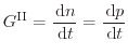
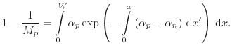
In the drift-diffusion model, the impact-ionization rate is usually expressed using the impact-ionization
coefficients ![]() and
and ![]() . These two coefficients describe the number of
electron-hole pairs generated per unit distance traveled [32] by a
solitary carrier between two collisions. Considering only electrons generated
by electrons, one can write
. These two coefficients describe the number of
electron-hole pairs generated per unit distance traveled [32] by a
solitary carrier between two collisions. Considering only electrons generated
by electrons, one can write
 |
(5.1) |
 |
(5.2) | |
 |
(5.3) |
![\includegraphics[width=0.6\textwidth]{figures/ii_fielddep}](img334.png)
|
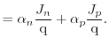
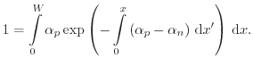
To describe the impact-ionization caused avalanche breakdown, for example, in reverse-biased junctions, a macroscopic formalism called ionization integral is introduced. This quantity is based on the impact-ionization coefficients. It considers carriers which enter the depletion region and are then accelerated by the electric field. The carriers gain enough energy to generate new electron-hole pairs by impact-ionization. If these newly generated carriers have high enough energy they can launch a secondary branch of impact-ionization. Therefore, the entire process can be cascaded, leading to avalanche carrier multiplication. This results in high currents and eventually leads to breakdown.
For a one-dimensional consideration, a depletion region with width ![]() is
assumed. An initial hole current density at the position of
is
assumed. An initial hole current density at the position of ![]()
![]() is considered to trigger the avalanche. The density
is considered to trigger the avalanche. The density ![]() steadily increases throughout the depletion region due to the holes generated
by impact-ionization as shown in Fig. 5.3(a).
steadily increases throughout the depletion region due to the holes generated
by impact-ionization as shown in Fig. 5.3(a).
The simultaneously generated electrons are accelerated in the opposite
direction resulting in an electron current density ![]() In steady-state, the
total current density
In steady-state, the
total current density ![]() defined as
defined as
| (5.6) |
| (5.7) |
|
Obtaining the numerical solution using this approach saves a lot of computational power. However, due to severe simplifications required to compute this integral, this method is not relevant for real devices. An important application field of the ionization integral is the measurement of the ionization rate. The latter quantity is not achievable in direct measurements, and thus the ionization integral can be used to conclude on the ionization rate using breakdown conditions.
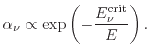
![$\displaystyle J_p(x) = J \exp \left( \int_0^x \left( \ensuremath{\alpha _p}- \e...
...h{ \mathrm{d}}x' \right) \ensuremath{ \mathrm{d}}x + \frac{1}{M_p} \right ] .$](img349.png)

![\includegraphics[height=69mm]{figures/ionizationintegral_current_html}](img355.png)
![\includegraphics[height=69mm]{figures/ionizationintegral_alpha}](img356.png)